Please select your location and preferred language where available.
Technology Topics
Introducing the latest technologies being researched and developed at KIOXIA Corporation and various use cases of flash memories.
-
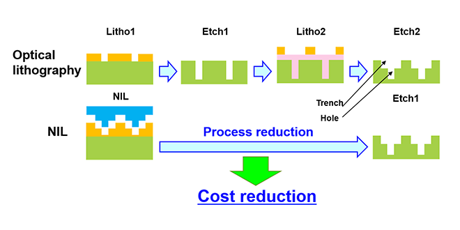
3D patterning is a unique feature of Nanoimprint lithography (NIL). We have studied fabrication of 3D dual-damascene structure using NIL. By optimizing the resist material, template structure, NIL conditions, and etching conditions, respectively, we succeeded in fabricating 3D dual-damascene structure with L/S=4X/4Xnm.
-
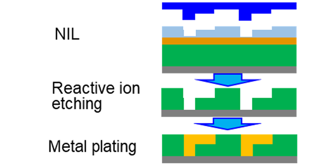
Two design constraints are introduced to improve process margin of Ultraviolet nanoimprint lithography. One is for NIL alignment mark design rule and the other is for pattern coverage rule with wafer topography.
-
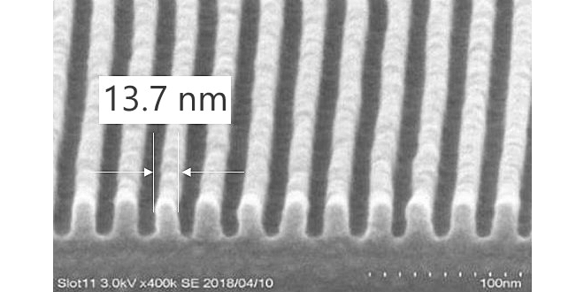
The accuracy of alignment with the underlying layer in UV nanoimprint lithography has been improved by using a method of making separate alignment marks. This enables the practical realization of low-cost patterning with a half-pitch of 14 nm in a single patterning step, which is impossible by optical lithography.

-
In order to cope with shrinking of semiconductor device pattern dimension below 30nm half pitch and increasing fabrication cost, we are developing low cost Nanoimprint Lithography (NIL.)
-
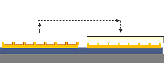
In order to overcome the lithography process cost increase, we are developing nanoimprint lithography that can miniaturize devices at lower cost.
R&D Organization

We aim to pursue continuous technological exploration and its social implementation to achieve an affluent and sustainable digitalized society through innovative memory technologies.

Conducts R&D on BiCS FLASH™, a type of 3D flash memory that KIOXIA was the first to develop in the world, while serving as a bridge between R&D and volume production.


