

Please select your location and preferred language where available.

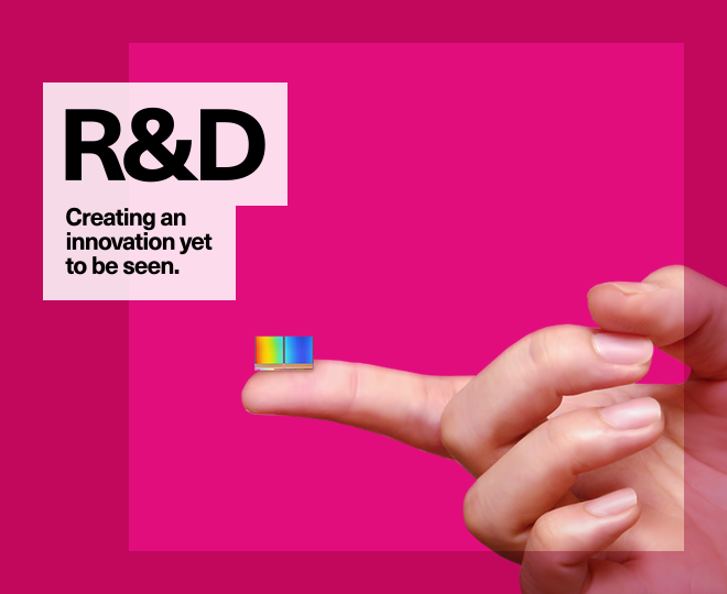
As a leading company in flash memory and SSD, KIOXIA delivers products that create new value. Research and development into cutting-edge technologies in many diverse fields is essential for realizing this. We implement technological innovation to pursue the potential of “memory.”
News
-
September 28, 2026 KIOXIA Updates
-
July 15, 2026 KIOXIA Updates
-
April 22, 2026 KIOXIA Updates
Kioxia’s Research and Technology Development

Chief Technology Officer, Hideshi Miyajima
Kioxia conceived and developed the world’s first NAND flash memory and 3D flash memory BiCS FLASH™, and we remain committed to promoting research and development in the future in order to realize our mission of “Uplifting the world with memory.”

Kioxia is committed to the development of engineers and supports individual career development from new employees to experienced engineers. Among them, Senior Fellows, who are the pinnacle of specific technical fields, inherit advanced expertise and are committed to the development of semiconductor technology. Here are some of our Senior Fellows who are active in domestic and international academic societies.
KIOXIA has developed many “world-first” technologies, such as NAND flash memory and created innovation. As a leading company in “memory,” KIOXIA will continue to work on cutting-edge research and development to create innovation.

The Shining Sun and the Flash Memory for Storage
~ Principle of 3D Flash Memory Operation ~
The principle of 3D flash memory operation is explained with CG animation by contrasting it to the way the sun shines.
Technology and Innovation at KIOXIA

As a leading company in flash memory and SSD, KIOXIA conducts research and technology development that supports the information society.
Introducing the relationship between KIOXIA's technology and society, and the "technology" of flash memory, which is the basis of our technology.
Innovations Created by KIOXIA

We would like to introduce the newly developed CMOS directly Bonded to Array (CBA) technology, which achieves improved performance and cost reduction for 3D flash memory.
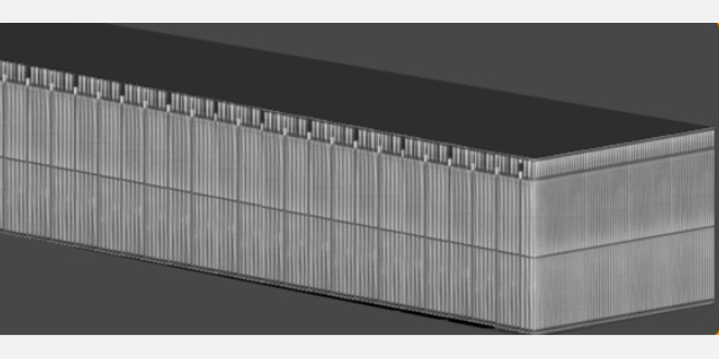
In 2007, KIOXIA was the first in the world to announce 3D flash memory technology. Here we present the key points of innovation that led to cost reductions and the initiatives for higher capacities, together with an explanation of BiCS FLASH™.
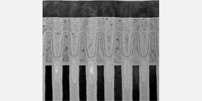
KIOXIA invented the world’s first NAND flash memory in 1987. This is an explanation of the structure of flash memory and the mechanism of data storage.
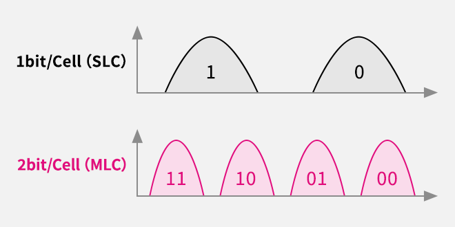
“Multi-level cell technology” is one of the main technologies realizing larger capacity flash memory. The 1 Gbit MLC NAND flash memory launched by KIOXIA in 2001 was the first application in the world of multi-level cell technology to a NAND flash memory product.
Technology Topics
Introducing latest technologies being researched and developed at KIOXIA Corporation and various use cases of flash memories.
-
We proposed a new cell structure with an ultra-thin metal/Si Hybrid Floating Gate (HFG) for horizontal channel flash, a candidate for future 3D flash memory. The Mo-based HFG exhibited significant improvements in program characteristics. This achievement was presented at the IMW 2026.

-
We proposed a novel approximate search method of activation-time-modulated sequential multi-block access for multi-level in-memory computing using 3D flash memory. We demonstrated approximate search using 3-bit and 128-dimensional key data with sufficient accuracy. This achievement was presented at the IMW 2026.

-
A 10th generation BiCS FLASH™ 2Tb 4bit/cell with a bit density of 37.6Gb/mm2 was developed. High-density design and new sensing techniques were implemented to achieve the world’s highest bit density chip among 4bit/cell products while delivering a high write throughput of over 85MB/s. In addition, this product utilized a new power reduction technique for super multi-stacked package.

KIOXIA's R&D Backgrounds
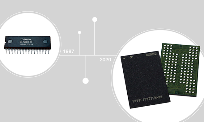
KIOXIA covers from R&D to mass production of flash memory and SSD products. Introducing the mechanisms of technological innovation, that is, how R&D is conducted in the process of bringing our products to market.
Introducing KIOXIA’s achievements in supporting the evolution of electric devices, such as the invention of NAND flash memory in 1987, and advancement of the information society on a global scale, seen through the lens of the history of memory and SSD development.
KIOXIA has been highly commended for the presentation of its R&D through a variety of channels, including major academic societies and research papers.
R&D Organization/Academic Collaboration
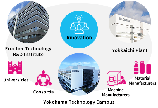
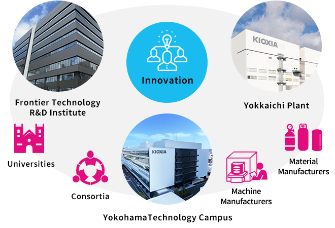
KIOXIA has established industry-leading R&D frameworks with “memory” technology. We use our various locations to conduct technological innovation while promoting open innovation.

To further accelerate the development speed and address the needs of increasingly diverse research themes, KIOXIA promotes R&D projects in collaboration with universities, technical communities, and research institutes both in Japan and abroad.


