Please select your location and preferred language where available.
Next-Generation Lithography Process: Nanoimprint
August 28, 2018
In the optical lithography process, shorter wavelengths and higher NAs that increase the lens diameter have been introduced to meet demand for device miniaturization. As wavelength reduction and NA heightening are approaching their physical limitations, new techniques are emerging, such as multiple patterning that repeats optical lithography several times or EUVL (Extreme Ultra-Violet Lithography). However, due to the cost of process step increase and additional process tools, it is inevitable that process costs will increase.
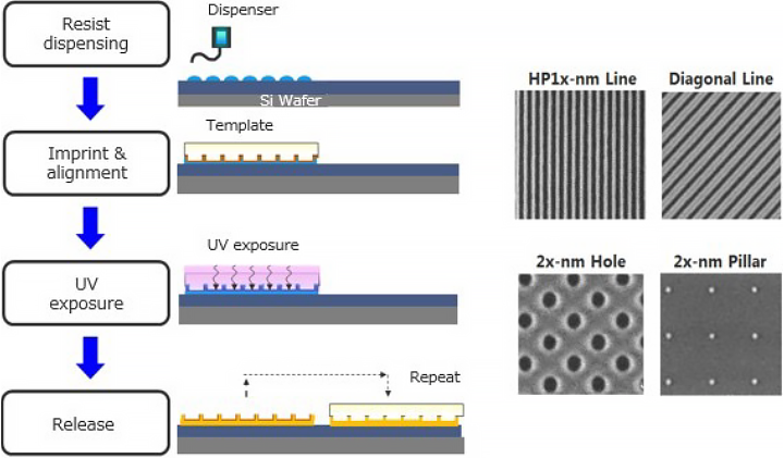
In order to overcome the lithography process cost increase, we are developing nanoimprint lithography that can miniaturize devices at lower cost. The nanoimprint technique uses imprinting to transfer nanoscale patterns on a template to a Si wafer, and unlike conventional lithography tools, it does not require a lens optical system for reduction projection.
The nanoimprint is a highly anticipated next-generation lithography method to realize advanced memory devices with reduced cost.


