Please select your location and preferred language where available.
What is the 3D Flash Memory “BiCS FLASH™”?
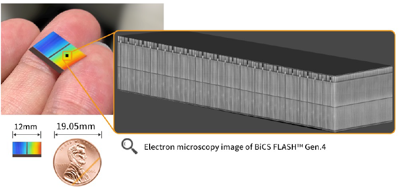
In 2007, KIOXIA was the first in the world to announce 3D flash memory technology. Here we present the key points of innovation that led to cost reductions and the initiatives for higher capacities, together with an explanation of BiCS FLASH™.
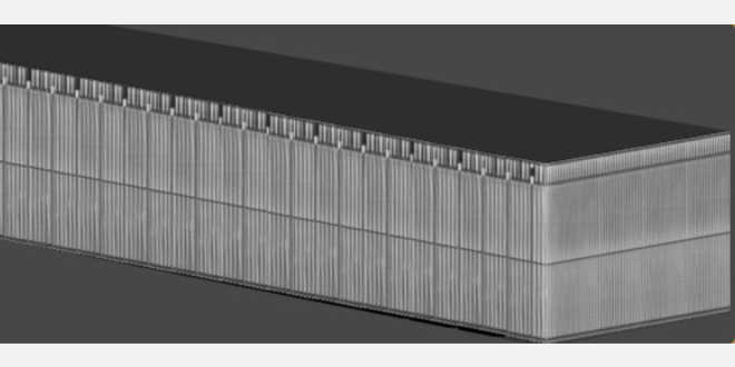
Increasing capacities in Flash Memory
The digitization of society is advancing rapidly and the amount of data that must be stored is increasing explosively. For this reason, it is necessary to increase capacity to store even larger amounts of data in a single flash memory.
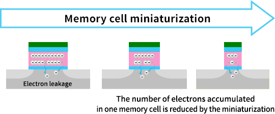
To achieve this large capacity, KIOXIA has developed technology for the miniaturization of memory cells, to reduce the area occupied by a single memory cell as much as possible so that as many memory cells as possible can be mounted in one flash memory product, and has realized the commercialization of 15 nm (nanometer*1) technology. However, there are limits to miniaturization technology. For example, the memory cells being close to each other leads to the phenomenon of unintended current flow. Also, as shown in Figure 1, the number of electrons accumulated in one memory cell is reduced by the miniaturization, so just very small electron leaks start to have an impact on the stability of the data.
- 1 nm (nanometer) is one billionth of a meter
The birth of BiCS FLASH™
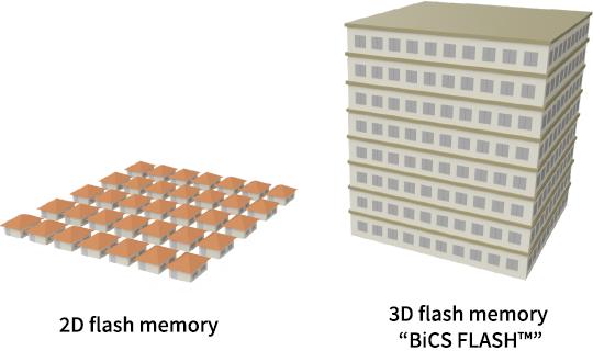
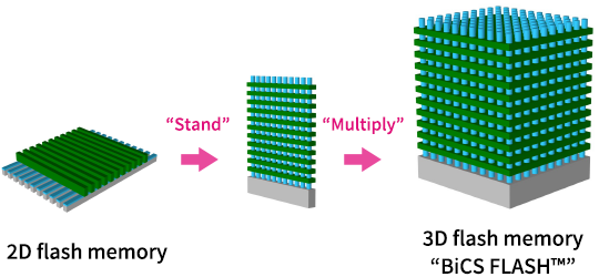
These issues led to the idea of increasing the number of memory cells per unit area by vertically stacking the planar structures of the flash memory. If we think of the example of a building, then this is like taking a one-story building where only 10 people can live and rebuilding it as a five-story apartment building where 50 people can now live in the same area of land. In other words, the higher the stacking is, the more people can live there without increasing the area of land (Figure 2).
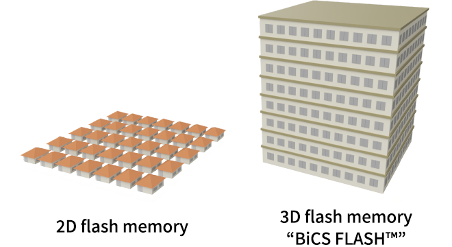
However, new issues were also created at that time. When the planar structure flash memory is stacked in order from the bottom, every time an additional memory layer is added, the work to create the flash memory structure also increases. In other words, the more the layers are stacked, the higher the cost is.
In response to this, KIOXIA announced the BiCS FLASH™ 3D flash memory in 2007 as a solution to this problem of the manufacturing cost.
Ever since presenting the concept of the “batch processing technology” of BiCS FLASH™ at an academic conference in 2007, BiCS FLASH™ products have been commercialized with 48 layers in 2015, 96 layers in 2018, 112 layers in 2020, and 162 layers in 2022, and the technology has been used in various products.

BiCS FLASH™ technology
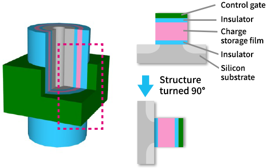
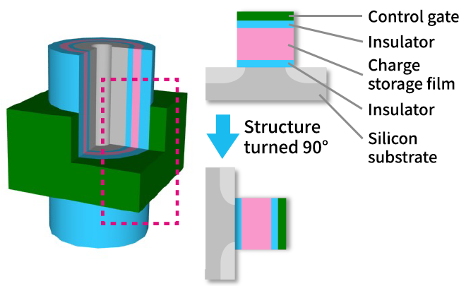
Here we explain the BiCS FLASH™ batch processing technology. With BiCS FLASH™, there is alternate stacking of a plate-shaped electrode that acts as the control gate (the green plates on Figure 4) and an insulator, and then a large number of holes are all opened up (punched) at once perpendicular to the surface. Next, the inner parts of the holes opened up in the plate-shaped electrodes are filled (plugged) with a charge storage film (the part shown in pink) and column-shaped electrodes (the column structures shown in gray). Under this condition, the intersection between the plate-shaped electrode and the column-shaped electrode is one memory cell.
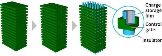
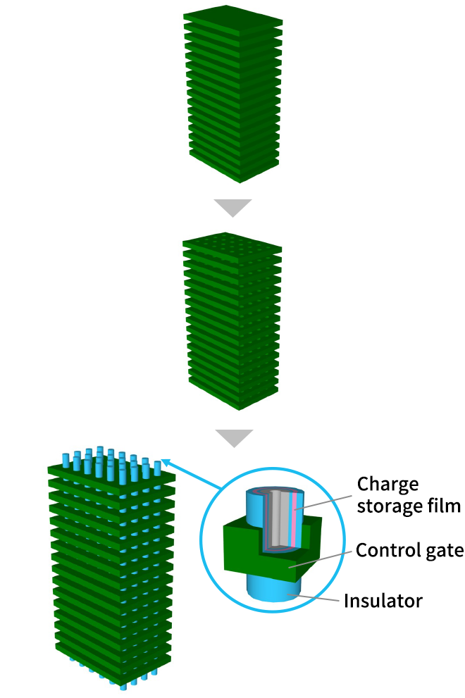
Let’s look at a magnified view of the BiCS FLASH™ memory cell (Figure 5). In a BiCS FLASH™ memory cell, electrons are exchanged between the electrode that passes through the center of the column (the structure shown in gray) and the charge storage film (pink).
In this way, rather than stacking up the memory cells one layer at a time, first the plate-shaped electrodes are stacked and then a hole is opened up through them and the electrodes are connected so that the memory cells are formed for all the layers all at once to reduce manufacturing costs. This groundbreaking technology is called BiCS FLASH™.
For even larger memory capacities
Furthermore, to achieve even larger memory capacities, KIOXIA has been continuing R&D to increase the number of layers for more than 10 years. As of March 2023, the stacking of more than 200 layers has been realized.*2 If we imagine the plate-shaped electrodes being stacked and the holes being opened through them to pierce the electrodes all at once, all in the realm of nanometers, then we can see how this BiCS FLASH™ is an extremely precise and delicate technology.
*2 The press release issued on March 30, 2023
