Please select your location and preferred language where available.
Advanced Memory Development Center
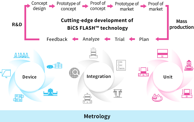
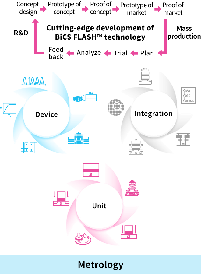
The Advanced Memory Development Center (AMDC) is committed to the development of BiCS FLASH™, a 3D flash memory. The role of the AMDC is to provide a bridge between research and mass production of next-generation products. To meet the growing demand for memory devices, it is necessary to reduce development time for high-capacity, high-speed, and low-power-consumption memory devices and accelerate time-to-market.
The AMDC is devoted to creating conceptual designs of new products through discussions with various divisions. Prototyping and verification are repeated at Yokkaichi Plant in order to establish manufacturing processes. In parallel with these tasks, the AMDC plans and implements technological development projects while optimizing evaluation technologies to enhance productivity.
The AMDC consists of three major development departments: 1) the Unit Process Department develops unit processes, 2) the Process Integration Department integrates unit processes to develop new device structures, and 3) the Device Department is responsible for taking the initiative in product development and improving device performance and yield. Metrology supports these processes by inspecting, measuring, and analyzing defects. These departments cooperate with one another in experimentation and data analysis to facilitate development while holding extensive discussions.
Departments
Unit Process
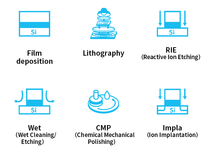
The Unit Process Department is committed to the establishment of various manufacturing processes necessary for memory development. Circuit patterns are transferred onto the wafer through thin-film deposition and optical lithography exposure. Manufacturing processes are supported by various fundamental technologies, including nanofabrication technologies such as plasma-based reactive ion etching (RIE) and wet cleaning and etching; chemical mechanical polishing (CMP), i.e., a polishing process combining chemical and mechanical forces; and ion implantation. The Unit Process Department is responsible for the conceptual design of these fundamental technologies necessary to realize the next-generation device structure; the evaluation and verification of manufacturing machines and materials based on the conceptual designs; and productivity improvement. For process development, the Unit Process Department collaborates not only with internal parties but also with material and manufacturing machine manufacturers.

Technology examples of the unit process department

Process Integration
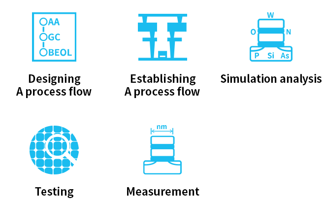
The Process Integration Department designs a process recipe to realize the structures of next-generation devices. Its role is to establish the optimum manufacturing process flow through repeated prototype experimentation and simulation. The structures of prototype devices are analyzed using state-of-the-art testing and measuring technologies compatible with new structures. The Process Integration Department is committed to process verification to establish manufacturing process flows with high reliability and productivity.

Role examples of the process integration department

Device
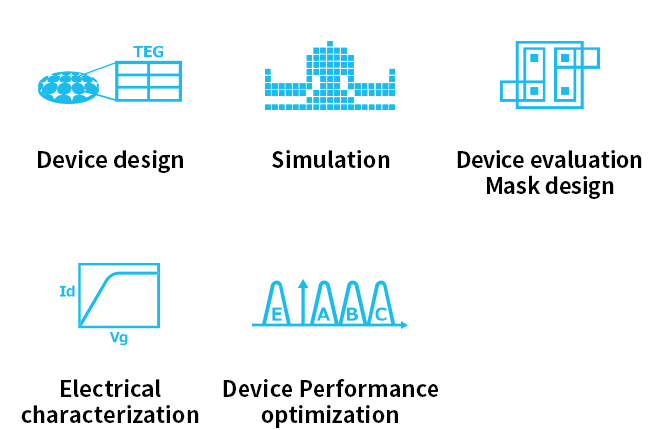
The Device Department designs devices for the next-generation products as well as the final products by integrating these devices. The electrical characteristics of evaluation devices called TEGs*1 and products are optimized through repeated computer simulations using TCAD*2 tools and prototype experiments. In the event of any failure being detected in the TEG or product, the Device Department identifies its causes through electrical and physical analysis and seeks solutions in cooperation with the Unit Process and Process Integration Departments. The Device Department coordinates entire development projects and establishes mass-production technologies for next-generation products.
- TEG:Test Element Group
- TCAD:Technology Computer Aided Design

Role examples of the device department

Open Innovation
To facilitate product development, the Advanced Memory Development Center (AMDC) not only participates in consortia and academic societies worldwide but also collaborates with universities and machine and material manufacturers in joint development projects. Engineers at the AMDC have inquiring minds and a passion for innovation, and possess diverse specialties. They are endeavoring to commercialize BiCS FLASH™ and other cutting-edge memory devices.
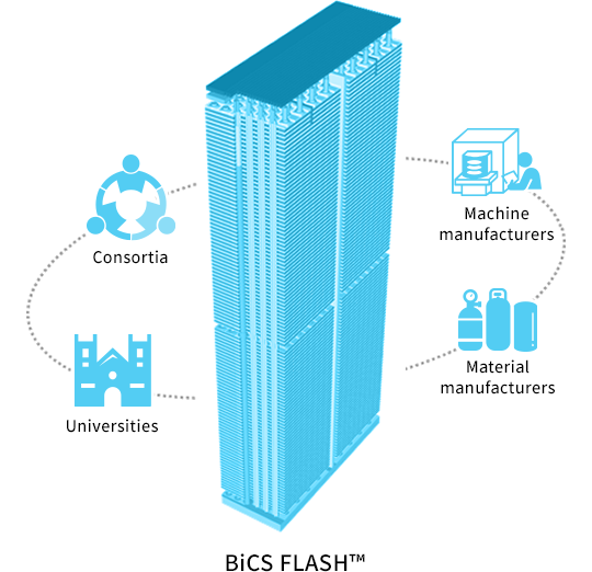
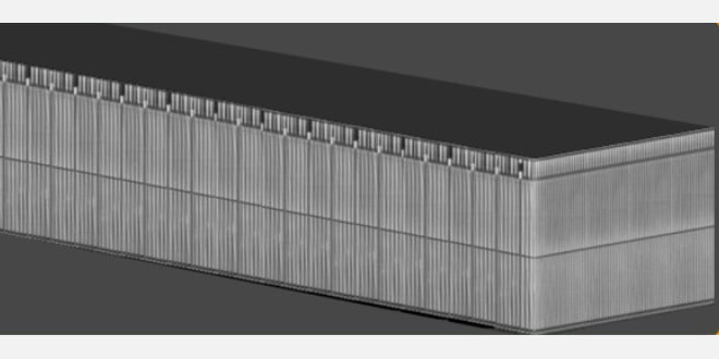
In 2007, KIOXIA was the first in the world to announce 3D flash memory technology. Here we present the key points of innovation that led to cost reductions and the initiatives for higher capacities, together with an explanation of BiCS FLASH™.
Related Technology Topics
-
As the number of word lines increases in 3D flash memory, erase speed degradation is expected to become a significant issue. In this work, we propose a novel Schottky source junction that drastically enhances erase operation. The proposed structure was experimentally demonstrated using a prototype cell array. These results were presented at the 2025 IEEE Symposium on VLSI Technology and Circuits.

-
We proposed the new architecture, Horizontal channel flash, which enables further cost reduction for future 3D flash memory. We also examined its cell characteristics and confirmed 10k cycle program/erase operations on a test device. This achievement was presented at the IEDM 2024.
