Please select your location and preferred language where available.
Design process integration enabling the productivity enhancement for nanoimprint lithography
October 5, 2022
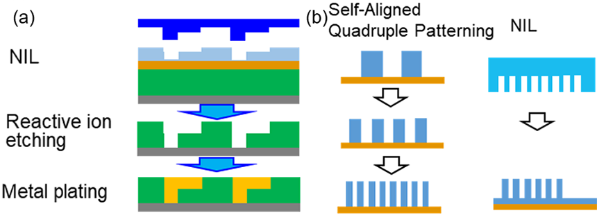
Ultraviolet nanoimprint lithography (NIL) is a simple contact process that is attractive and promising process for high pattern fidelity, without blurring effect due to light scattering or acid diffusion in the resist. Specifically, complicated 3D patterns, fine 2D patterns, and fine 1D patterns can be formed in fewer process steps compared to those for optical lithography. (Fig. 1)

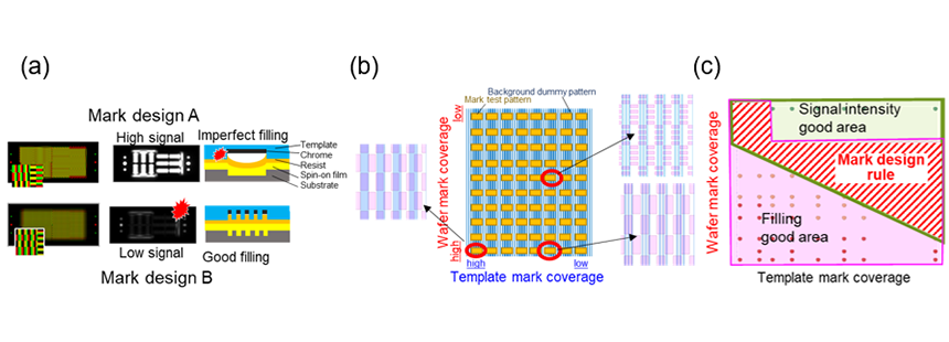
On the other hand, there are fewer adjustment knobs for process tuning in NIL; therefore, it is necessary to introduce design restrictions customized for NIL to improve the process margin. Since pattern transfer is performed through filling of a resist having a finite volume, a design constraint considering filling property is required to reduce defect density and improve throughput. In this study, two types of design constraints are examined to address the NIL process margin problem. One is a NIL alignment mark design that satisfies both signal strength and filling characteristics. The other is a combination of the pattern coverage rule with wafer topography that achieves good filling characteristics under various substrate unevenness conditions. Experiment results were interpolated with NIL process simulations and common areas under various conditions were extracted to identify the design rules for achieving large process margins. (Fig. 2)

By using a design flow that considers these rules, we believe that high volume manufacturing (HVM) yields can be increased considerably by reducing yield issues and reducing redesign loops.
This technique was presented at the SPIE AL (society of photo-optical instrumentation engineers advanced lithography) on demand at May 2022.
This article is based on the quotes from the references [1], and edited accordingly.
Reference
[1] Sachiko Kobayashi, Satoshi Mitsugi, Katsuyoshi Kodera, Kazuya Fukuhara, Anupam Mitra, Koki Ueha, Katsuya Abe, Motofumi Komori, Shingo Kanamitsu, Takuya Kono, “Design process integration enabling the productivity enhancement for nanoimprint lithography”, Proc. SPIE 12052, DTCO and Computational Patterning; 1205208 (2022) © 2022 Society of Photo Optical Instrumentation Engineers (SPIE).

