Please select your location and preferred language where available.
14nm Half-pitch Direct Patterning with Nanoimprint Lithography
March 17, 2020
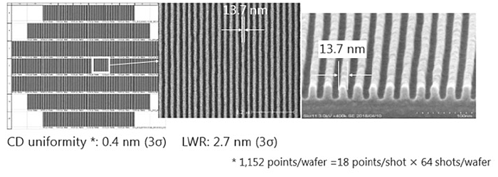
In order to cope with shrinking of semiconductor device pattern dimension below 30nm half pitch and increasing fabrication cost, we are developing low cost Nanoimprint Lithography (NIL) (Please refer to the article ”Next-generation lithography (NGL) process: Nanoimprint” on this home page). We have fabricated 14 nm half-pitch template using self-aligned double patterning (figure 1) method. Using this template, we have successfully fabricated 14 nm half pitch resist pattern (figure2) as well as Si lines (figure 3) on a 300 mm wafer. Thus, we have been able to demonstrate that the NIL is a promising NGL candidate for future miniaturized devices and has a potential for lowering the fabrication cost by reducing the number of process steps.


Since NIL needs direct contact of the fine pattern template and wafer, increasing the template life i.e., reducing potential damage to the template, improving throughput by promoting faster resist filling into the template features and, achieving high overlay accuracy by controlling template distortion, are the problems to be solved. We have demonstrated, long template life by developing technologies for in-situ particle removal from the template (figure 4), high throughput by developing new resist and gas permeable spin-on-carbon (GP-SOC) for faster resist filling (figure 5) and, high overlay accuracy using technology to control high order distortions (figure 6).


We presented these achievements at SPIE Advanced Lithography Conference in San Jose, USA in February 2019 [1].
Reference
[1] T Kono, M. Hatano, H. Tokue, H. Kato, K. Fukuhara, and T. Nakasugi, “Half pitch 14nm direct patterning with Nanoimprint Lithography”, Proceedings of SPIE - The International Society for Optical Engineering, 10958 (2019)

