Please select your location and preferred language where available.
Evaluation of alignment accuracy for nanoimprint lithography
October 5, 2022
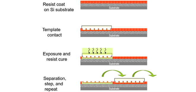
UV nanoimprint lithography (hereafter referred to as NIL) is a process in which a mask and a silicon substrate are in direct contact with each other to transfer the original plate pattern onto the substrate as shown in Figure 1.
Unlike optical lithography, resist patterns are formed on the wafer at the same scale as the original template pattern. The template pattern, originally created by electron beam lithography, can be formed with dimensions in the 10 nm range. The template pattern was originally created by electron beam lithography. As reported in the past [1-3], NIL produces half-pitch 14 nm line-and-space patterns in a single patterning step, which exceeds the resolution limit of optical lithography. In this presentation, we report on the alignment performance of NIL with the underlying pattern [4].
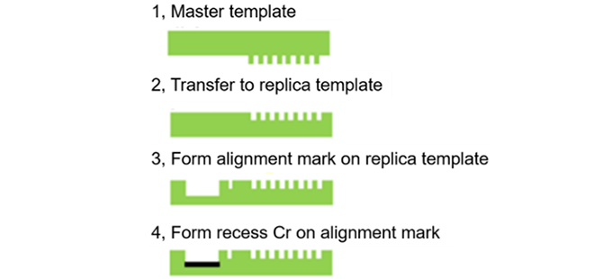
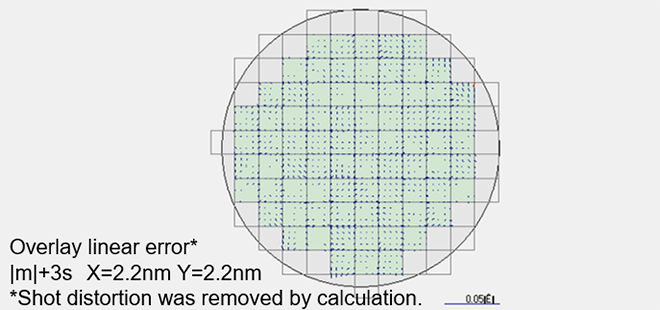
Although NIL has achieved a substrate alignment accuracy of 2 nm, it has problems specific to particularly fine patterning, such as a half-pitch of 14 nm: The design constraints of the template manufacturing process cause the alignment signal to become lower during alignment of the template to the Si wafer, resulting in poor alignment reproducibility. In this study, we improved the alignment signal by using a different manufacturing process for the NIL alignment marks formed on the template surface, such as using a separate process for the device pattern and alignment marks as shown in Figure 2, and actually demonstrated that the alignment and imprinting on the silicon substrate can be achieved as shown in Figure 3.


Furthermore, we experimentally demonstrated that sufficient alignment signal intensity and alignment accuracy can be obtained using multiple types of substrates that simulate device structures. This achievement proceeds the way for cost reduction in advanced memory device manufacturing through half-pitch 14nm single patterning and high-precision alignment with the underlying pattern for actual use.
This article is a partial excerpt and reconstruction of drawings, etc., from Ref. [4].
Reference
[1] T. Nakasugi et al., “Half pitch 14 nm direct pattering with Nanoimprint lithography”, 2018 IEEE International Electron Devices Meeting (IEDM), IEDM Technical Digest 2018, pp. IEDM18-265-268.
[2] T. Kono et al., “Half pitch 14nm direct patterning with Nanoimprint Lithography”, Proc. SPIE, 2019, 10958, 109580H.
[3] T. Nakasugi et al., “Multi-field imprint technology: enabling the productivity enhancement of nano-imprint lithography”, J. of Micro/Nanopatterning, Materials, and Metrology, 21(1), 011002 (2021).
[4] K. Fukuhara et al., “Evaluation of alignment accuracy for nano-imprint lithography”, SPIE Advanced Lithography + Patterning 2022 On Demand, May 23-29, 2022.

