Please select your location and preferred language where available.
7-bit per Cell Demonstration of 3D Flash Memory by Combination of Single-crystal Channel and Cryogenic Operation
October 5, 2022
The global data sphere, a term used to describe the entire quantity of digital data generated every day worldwide, is predicted to reach 175 ZB by 2025. Currently, these massive amounts of data are stored on high-capacity servers and in data centers, which primarily use HDDs and SSDs. In addition, SSDs outperform HDDs in data read/write speed, power usage, and device size. And they are replacing HDDs. This has been realized by the continuous bit-cost scaling of flash memory. Bit cost scaling of flash memory is attributed to stacking memory cells in more layers in the 3D direction and storing more signal levels, i.e. more bits in a single memory cell.
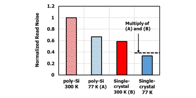
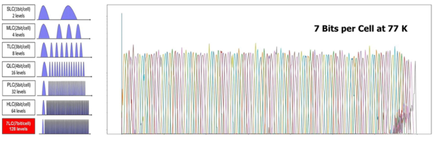
In a previous article, we discussed how BiCS FLASHTM (3D flash memory) performed at cryogenic temperatures and demonstrated a 6-bit per cell with better storage performance.[1, 2] This time, by combining cryogenic operation with silicon process technology that can improve memory cell characteristics, we have advanced one step and successfully demonstrated the world’s first 7-bit per cell. The traditional poly-silicon used for the channel of the memory cell transistor was replaced by single-crystal silicon. (Fig.1) In the read operation, the threshold voltage (Vth) of memory cell is determined and converted into bit information, but there is a fluctuation in Vth called the read noise. Cryogenic operation and single-crystal channel can greatly minimize read noise. (Fig.2) As a result, it is easier to achieve larger multi-levels in a cell. In a single memory cell with 7-bit per cell, 128 (27) Vth distributions can be created. (Fig.3) The highest multilevel flash memory cell in mass production is the 4-bit per cell. Our proposed 7-bit per cell is expected to significantly lower the bit cost, including the additional cryogenic cooling cost.
At the Kioxia laboratory, we continue to develop low-temperature memory technology that cools and operates at cryogenic temperatures to achieve the lowest bit cost and to enable continuous bit-cost scaling with silicon technology in the future.


This research has been presented at the International Memory Workshop (IMW) in May 2022.[3]
This article is reconstructed from excerpts of references[3] @IEEE.
Reference
[1] Y. Aiba, H. Tanaka, T. Maeda, K. Sawa, F. Kikushima, M. Miura, T. Fujisawa, M. Matsuo, and T. Sanuki, ” Cryogenic Operation of 3D Flash Memory for New Applications and Bit Cost Scaling with 6-Bit per Cell (HLC) and beyond”, 2021 5th IEEE Electron Devices Technology and Manufacturing Conference, EDTM 2021, 9421051
[2] T. Sanuki, Y. Aiba, H. Tanaka, T. Maeda, K. Sawa, F. Kikushima, and M. Miura, “Cryogenic Operation of 3-D Flash Memory for Storage Performance Improvement and Bit Cost Scaling,” in IEEE Journal on Exploratory Solid-State Computational Devices and Circuits, 2021, vol. 7, no. 2, pp. 159-167
[3] H. Tanaka, Y. Aiba, T. Maeda, K. Ota, Y. Higashi, K. Sawa, F. Kikushima, M. Miura, and T. Sanuki, “Toward 7 Bits per Cell: Synergistic Improvement of 3D Flash Memory by Combination of Single-crystal Channel and Cryogenic Operation,” 2022 IEEE International Memory Workshop (IMW), 2022, pp. 1-4

