Please select your location and preferred language where available.
Development of the new architecture, Horizontal channel flash, for future generations of 3D flash memory
March 5, 2025
3D flash memory venders have reduced its gigabyte cost by increasing the number of stacking layers for higher cell density. However, the limits of cost reduction and the degradation of cell current, which is related to read operation speed, were pointed out as critical issues that must be overcome for future generations with a large number of stacking layers[1]. From this point of view, we have proposed and demonstrated the new architecture, Horizontal channel flash (hereafter called HCF), as a candidate for next generation’s 3D flash memory[2].
As shown in Figure 1, HCF consists of a cell area, a staircase area, and a structure called LBI (Local Block Interconnect) that connects them. The cell is the structure where data is stored, the staircase is the connection area where the data stored in the cell is sent to the outside as electrical signals, and the LBI is the metal wiring that electrically connects them. Unlike conventional 3D flash memory, the channels are formed in the horizontal direction (XY plane) to the substrate, not in the vertical direction (Z direction). This structure is beneficial for HCF from the viewpoint of cell current. Its cell current does not decrease even in future generations with a large number of stacking layers because the cell current is independent of the number. In the cell area, data storage cells are formed at the crosspoint of the channel (XY plane) and word line (Z direction).
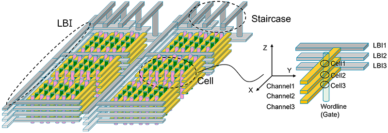
It consists of a cell area, a staircase area, and metal wirings (LBI) connecting them ©2024 IEEE[2]
Figure 2 shows the top view of the cell area in Figure 1. For each channel, Floating Gate (FG) cell and Select Gate (SG) are formed on both left and right sides. The SGs are electrical switches that select which channel is used and the FG cells store data. Since cells are formed on both sides of the channel, their density becomes higher than the conventional 3D flash memory. Thus, there is a possibility of cost reduction compared to conventional 3D flash memory.
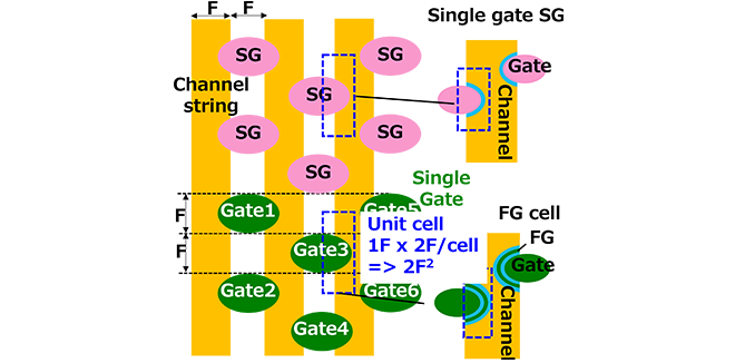
Cells are formed on both sides of a channel (orange) placed vertically in the image ©2024 IEEE[2]
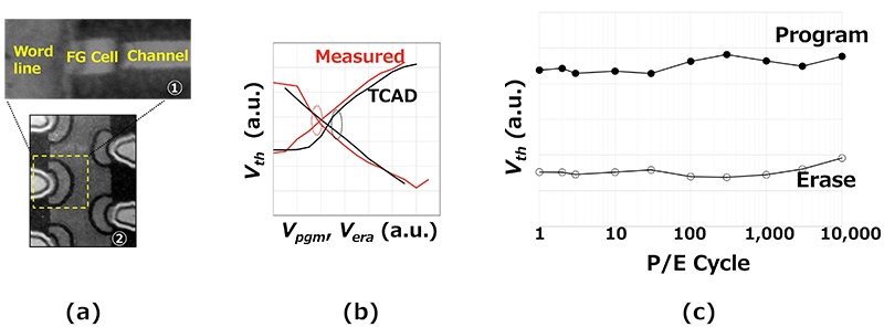
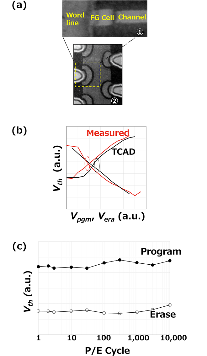
We fabricated a test sample of HCF and examined its Program/Erase operation characteristics. Figure 3(a) shows a cross-sectional TEM (Transmission Electron Microscope) image of the FG cell. It can be seen that the FG cell is successfully formed between the word line and the channel. Program/Erase characteristics of the cell on an actual device is compared to TCAD (Technology Computer Aided Design) simulation in Figure 3(b). We confirmed that the threshold voltage, Vth, is changed by the Program/Erase pulse as predicted by the simulation. Furthermore, as shown in Figure 3(c), Vth window does not degrade even after 10,000 Program/Erase operations, showing that the cell has high endurance against Program/Erase cycle operation.
As described above, we are pioneers in verifying the operation of HCF, which has the potential for further cost reduction. We will continue the feasibility study of HCF.
This achievement was presented at the IEEE IEDM 2024 (IEEE International Electron Devices Meeting 2024).
Reference
[1] R. Katsumata, “Overview in three-dimensionally arrayed flash memory technology”, in Short Course. 2019 Symposium on VLSI Technology and Circuits
[2] M. Oda et al., “Superior Scalability of Advanced Horizontal Channel Flash for Future Generations of 3D Flash Memory”, in Proc. 2024 IEEE International Electron Devices Meeting (IEDM)

A technical glossary that covers terms related to KIOXIA products and technologies, such as memory and SSDs. We explain that it can be used by engineers and researchers to the general public.

KIOXIA has established industry-leading R&D frameworks with “memory” technology. We use our various locations to conduct technological innovation while promoting open innovation.