Please select your location and preferred language where available.
Demonstration of Accelerated STT-Switching and High Retention in a 14nm MTJ towards High-Density STT-MRAM
March 14, 2024
Latest innovative technologies like AI, IoT, and deep learning increase demands for high-speed non-volatile memory with much higher density and lower cost as compared to conventional DRAM. Spin-Transfer-Torque(STT) -MRAM using perpendicular magnetic anisotropy is a promising candidate for high-density standalone-MRAM. Toward much higher density, higher speed, and lower cost STT-MRAM, further sustainable MTJ scaling to 1Z (Z=4-5) nm is strongly required. However, a conventional MTJ using a CoFeB single storage layer has the difficulty in 10-years retention below ⁓20nm. We have proposed a novel 14nm MTJ design and demonstrated high retention and high-speed writing simultaneously towards 1Znm STT-MRAM.
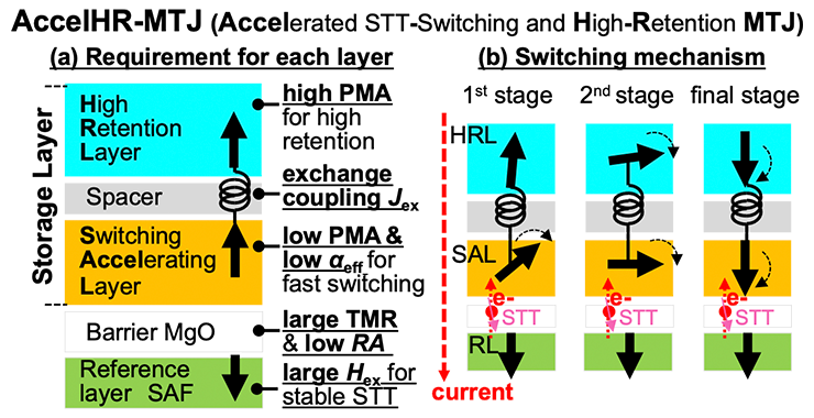
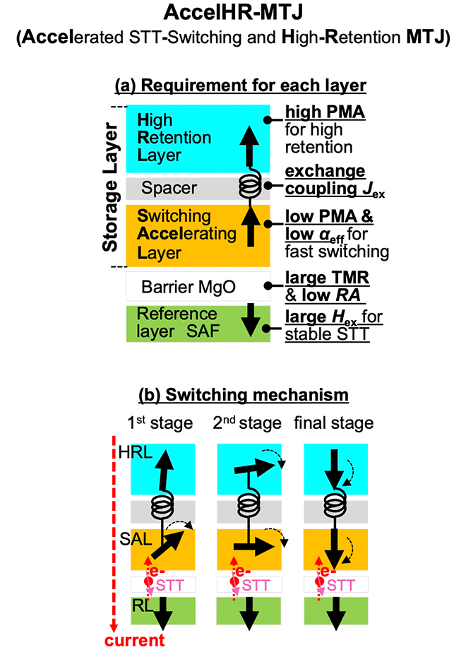
Key design concept of our MTJ, called as AccelHR-MTJ(Accelerated STT-Switching and High-Retention MTJ), is to assign the functions of high retention and high-speed writing to separate magnetic layers in a storage layer (Fig.1(a)), where PMA denotes perpendicular magnetic anisotropy, Jex is exchange coupling, αeff is effective damping constant, RA is resistance-area-product, and Hex is exchange coupling field of synthetic antiferromagnetic-reference layer(SAF-RL), respectively.
AccelHR-MTJ consists of a high-retention layer(HRL) with high PMA for high information retention capability, a switching accelerating layer(SAL) with low PMA and low αeff for high-speed STT switching. Magnetizations(M) in HRL and M in SAL are ferromagnetically coupled by Jex between HRL and SAL. Figure 1(b) shows a schematic switching mechanism of AccelHR-MTJ. First, magnetization of SAL is tilted rapidly by STT. Then, magnetization of SAL layer makes tilting of magnetization of HRL by the exchange coupling, like spring. Finally, magnetization of HRL is rapidly switched.


To demonstrate the concept of AccelHR-MTJ, we have created a multilayer film stack according to the design concept. The film stack of AccelHR-MTJ were successfully patterned into very small MTJs down to diameter of 14nm using a low-edge damage microfabrication technique based on ion beam etching (Figure 2).

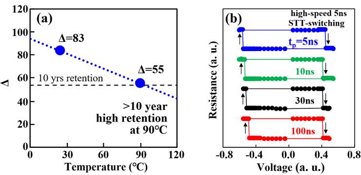
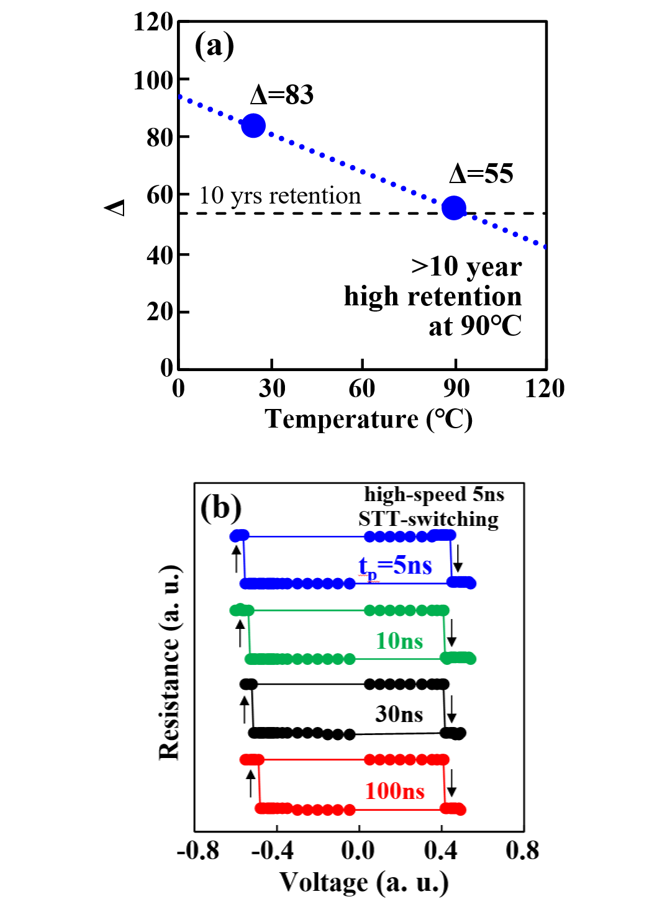
Figure 3 shows the high thermal stability factor (Δ) for high retention and high-speed writing characteristics obtained in the same 14nm AccelHR-MTJ device. Note that, high retention of >10 years and high-speed STT-switching at writing pulse width (tp) of 5ns are simultaneously achieved in our 14nm AccelHR-MTJ as predicted by its design concept. These results demonstrate that AccelHR-MTJ has the potential for high-density, high-speed, and low-cost 1Znm STT-MRAM.


This achievement was presented at the IEDM 2023.
Reference
[1] M. Nakayama et al., 2023 International Electron Devices Meeting (IEDM), San Francisco, CA, USA, 31-1

