Please select your location and preferred language where available.
A Bridge Chip for Scalable Performance and Capacity Storage Systems
January 30, 2024
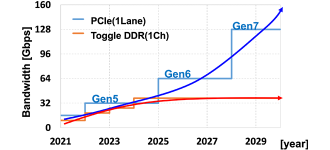
The growing demand for big data and cloud computing requires high-speed, high-capacity storage systems. While the speed of host interfaces(IFs), such as the PCIe® employed in SSDs, is steadily increasing, it is becoming more difficult to increase the IF speed of NAND Flash Memory(NAND) (Figure 1).
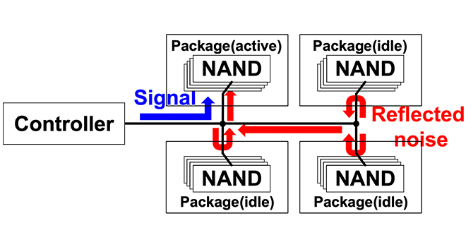
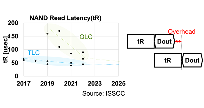
One reason of the difficulty is that signal integrity is degraded along with increase in IF speed. Especially, in case of a high capacity SSD, signal integrity is significantly degraded due to reflected noise from multiple packages with multi-stacked NAND dies which are in idle state (Figure 2(a)). The other reason is that only increasing the NAND IF speed does not produce higher throughput. The increased number of word line stack layers and multi-levels(3b/cell or 4b/cell[1]) of NAND tend to limit the reduction of the NAND read latency (tR). If the data output period(Dout) is smaller than the tR due to increasing the NAND IF speed, the read throughput is limited by the tR (Figure 2(b)).
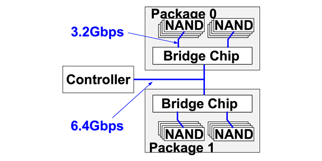
To solve these problems, the Bridge Chip with multi chip access is needed to keep up with the PCIe IF speed while maintaining the NAND IF speed. The developed Bridge Chip provides twice the NAND IF speed even with multiple packages on each PCB channel (Figure 3).
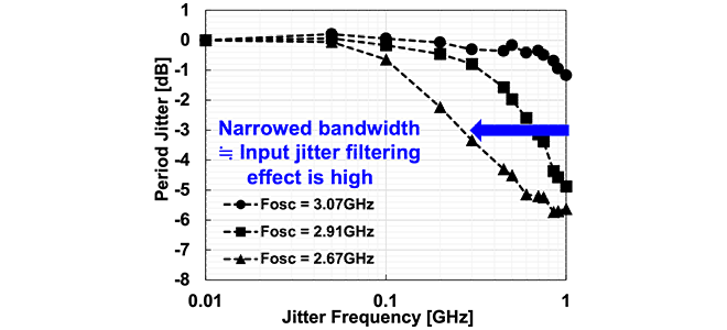
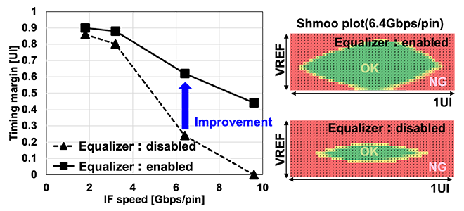
The Bridge Chip employs an Injection-Locked VCO-based PLL with high jitter filtering effect to improve the NAND IF performance and equalizers to compensate for reflected noise in multi-drop channel configuration. Injection-Locked VCO-based PLL greatly extends its pull-in range with injection current scheme at both the rising and falling edges of the input signal. Due to this wide pull-in range, the free-running frequency of the VCO(FOSC) can be initially set lower than that from the input CLK frequency(FCKIN), which leads to narrowing more the -3dB bandwidth of the input period jitter transfer function (Figure 4(a)). A 4-tap Decision Feedback Equalizer implemented in RX compensates the reflected noise and improves the EYE opening in 2-drop channel configuration (Figure 4(b)).
The Bridge Chip fabricated in a 12nm CMOS process is demonstrated at 6.4Gbps/pin with 2.85pJ/b I/O energy efficiency in a read operation. The NAND Multi-Chip Package(NAND MCP) incorporating the Bridge Chip and eight 1-Tb NAND dies achieves data transmission to and from FPGA at twice the speed of the NAND IF in a 2-drop channel configuration.
Twice the NAND MCP speed can reduce the wire area on PCB and the silicon area of Controller, which can lead to lower system cost. The techniques demonstrated in this paper enable the NAND MCP speed to increase even in the multi-drop channel configuration and realize the scalability of performance and capacity for the NAND storage system.
This achievement was presented at 2023 IEEE Asian Solid-State Circuits Conference(A-SSCC).
Reference
[1] J. Yuh, et al., “A 1-Tb 4b/Cell 4-Plane 162-Layer 3D Flash Memory with a 2.4-Gb/s I/O Speed Interface,” ISSCC, pp.130-132, Feb. 2022.

