Please select your location and preferred language where available.
New Evaluation Method for Nanomaterials
February 28, 2019
In order to realize new memory devices, development of nanomaterials (molecules or particles whose size is less than 10nm) is crucially important, but it is extremely difficult to evaluate their electrical properties.
For example, when the top electrode material is deposited on the nanomaterial on the bottom electrode, degradation of the nanomaterial may occur if the heat resistance of the nanomaterial is low, or a short between the top electrode and the bottom electrode may occur if the top electrode material penetrates the nanomaterial. Probing by STM (Scanning Tunneling Microscope) is another evaluation method, but it is very difficult to get good reproducibility.
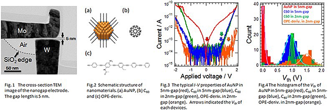
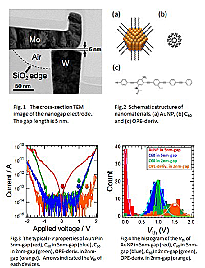
We have established a brand-new evaluation method for nanomaterials by applying the state-of-the-art semiconductor fabrication process. Firstly, a large number of nanogaps like one in Fig.1, whose space is almost the same size as the nanomaterial, are formed at once with good controllability, and then a nanomaterial is inserted into the nanogap. Figure 2 shows examples of nanomaterials, namely, a gold nanoparticle, fullerene C60, and an oligo-phenylene-ethylene derivative. Figure 3 shows I-V characteristics of nanomaterials in a 5nm or 2nm gap . Very small current, lower than 1pA (p=10-12), can successfully be measured. Figure 4 shows the histogram of the threshold voltage that can flow 0.1pA current, and distributions can be obtained by multi-point measurement.
We will continue to develop new evaluation methods and apply them in the development of new nanomaterials, and promote the development of new functional devices.


