Please select your location and preferred language where available.
Understanding of Polarization Reversal and Charge Trapping under Imprint in HfO2-FeFET by Charge Component Analysis
November 15, 2023
Ferroelectric field effect transistor(FeFET) has attracted attention as a candidate for emerging high-speed memory devices. FeFET is a transistor-type non-volatile memory that uses a ferroelectric film as the gate insulator. The direction of ferroelectric polarization can be controlled by the gate voltage, and the threshold voltage Vth of the transistor shifts by the polarization reversal. Especially, HfO2-FeFET, which uses HfO2 as a ferroelectric film, has the advantages of low-voltage, high-speed operation and CMOS compatibility.
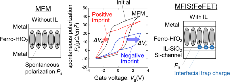
We focus on “imprint”, which is one of the critical reliability challenges in FeFET. Imprint is a phenomenon in which the gate voltage required for polarization reversal(coercive voltage Vc) shifts while the polarization state is maintained(Figure 1). In a capacitor structure (MFM*1), the spontaneous polarization Ps versus the gate voltage Vg(hysteresis) shifts to the left or right as a result of imprint. Since FeFET(MFIS*2) has a SiO2 interfacial layer(IL-SiO2) with low dielectric constant, it is necessary to consider not only the Vc shift due to imprint but also the change in the internal electric field due to interfacial trap charge. However, the measured charge generally contains both Ps and trap charge. Therefore, we separately extracted Ps and trap charge of FeFET experimentally and quantitatively by our original method[1], and clarified the imprint model in FeFET.
- Metal-Ferroelectric-Metal
- Metal-Ferroelectric-Insulator-Semiconductor

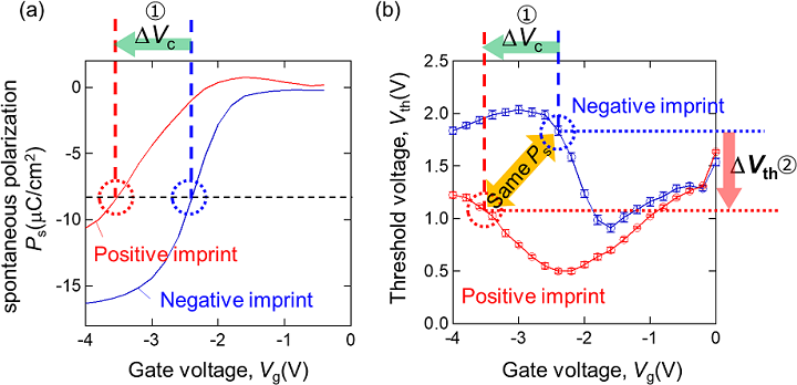
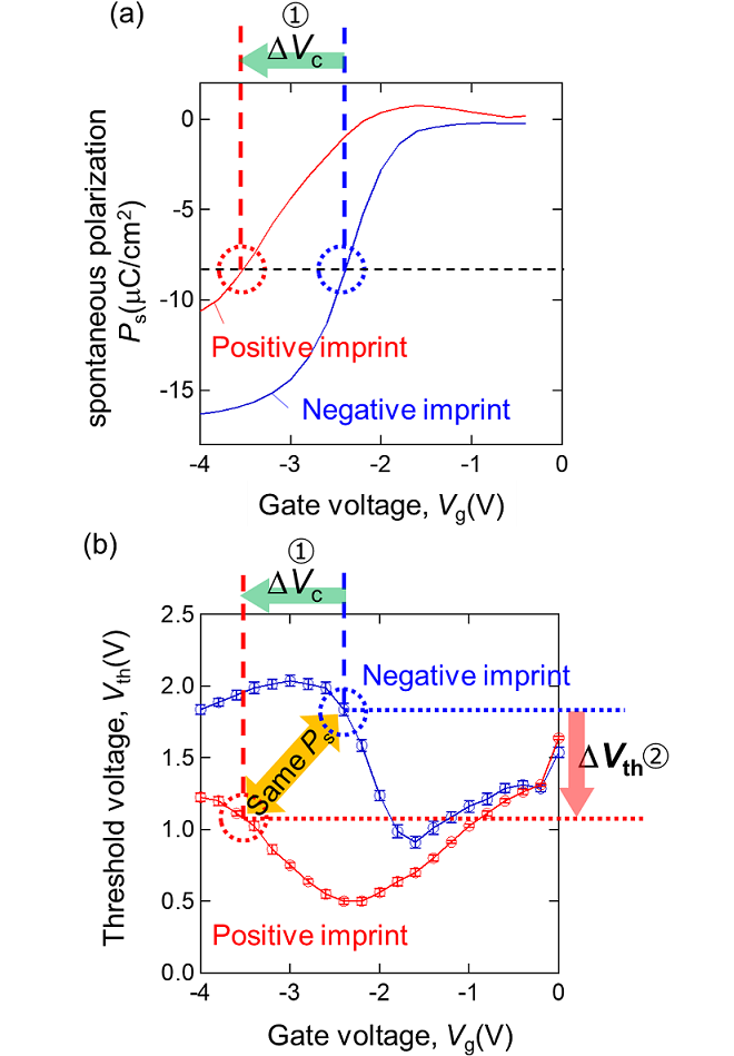
Figure 2(a) shows gate voltage dependence of Ps extracted by our original method[1] in MFIS. Vc, which yields the same Ps, shifts between the negative and positive imprint states, confirming the typical imprint behavior in the MFIS(①). Figure 2(b) shows gate voltage dependence of Vth in MFIS. Vth contains information on both Ps and trap charge. From Figures 2(a) and (b), we found that there is a Vth shift(②) in addition to a Vc shift(①) between the different imprint states. In this work, we found that the two imprint states take different Vth despite the same polarization in MFIS.


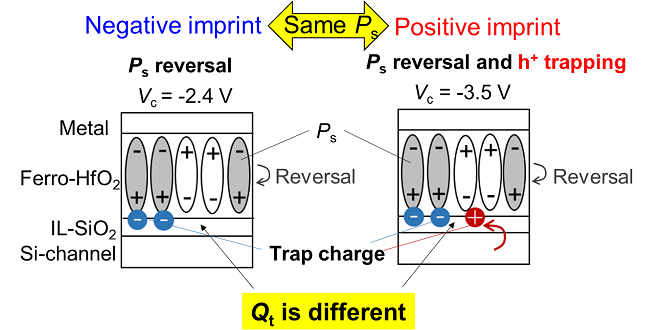
As mentioned above, the origin of the Vc shift(①) is the imprint observed also in the MFM. The reason for the difference in Vth(②) despite the same Ps can be explained by the difference in interfacial trap charges. Figure 3 shows a schematic diagram of the polarization state and trap charge for negative and positive imprint states at Vc. Absolute value of Vc for positive imprint state is higher than that for negative imprint state. By applying a higher absolute value of Vc, not only polarization is reversed, but also holes are trapped near the interface. Therefore, the negative and positive imprint states with different Vc change the charge trap density at the interface after erase. As a result, modulation of Vth is observed.

We found that Vth modulation due to trap charge occurs in addition to Vc shift due to imprint in FeFET. We believe that this result is a valuable knowledge to improve the reliability of FeFET.
This achievement was presented at 2023 SSDM(International Conference on Solid State Devices and Materials)[2].
This article is reconstructed from excerpts of references [2] ©2023 Japan Society of Applied Physics.
Reference
[1] R. Ichihara et al., VLSI2020, TF1.2.
[2] Y. Yoshimura, et al., Ext. Abstr. Solid State Devices and Material, 2023, p. 375.

