Please select your location and preferred language where available.
Comprehensive Analysis of Hole-Trapping in SiN Films with a Wide Range of Time Constants Based on Dynamic C-V
July 12, 2023
Charge trap memory is a non-volatile memory based on the threshold voltage (Vth) modulation of a transistor depending on the polarity and density of charges captured at traps in the gate dielectric. It is essential to understand not only long-term data retention characteristics but also Vth instability in short time domain. However, the short term characteristics of charge trap within 1 sec have been unclear.
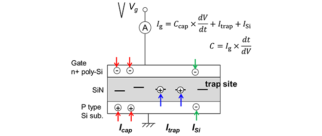
In this study, we newly developed an analysis method which can evaluate trap characteristics in a wide time range including short time domain such as 10µs. In this method, charge trapping and de-trapping are directly observed in addition to charging and discharging of MIS (Metal Insulator Semiconductor) capacitor (Figure 1).

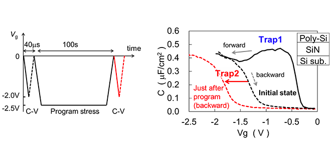
Based on this method, we clarified two types of traps in SiN. Figure 2 shows C-V (Capacitance-Voltage) characteristics of a MIS capacitor with SiN gate dielectric measured by newly developed method. Broad peak in forward sweep (solid line) of C-V curve (Figure 2) means that hole trapping (Trap1) occurs at low voltage of about -0.7V. Since this forward sweep takes about 10µs, it is suggested that Trap1 captures holes within short time domain. By applying longer program stress at higher voltage (-2.5V, 100s), the C-V curve shifts to negative (shift from black dashed line to red dashed line in Figure 2), indicating additional hole trapping. The existence of another type of trap (Trap2) which captured holes under higher voltage in longer time than Trap1 is clarified.

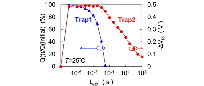
The characteristics of hole de-trapping from Trap1 and Trap2 are shown in Figure 3. Hole de-trapping from Trap1 starts in about 10µs and finishes within 30ms. On the other hand, de-trapping of all the holes from Trap2 takes a time longer than 1000s. It is clarified that both hole trapping and de-trapping of Trap1 are faster than that of Trap2.

In this study, we successfully observed the hole trapping and de-trapping in a wide time range including short time domain such as 10µs by using the newly developed analysis method. Such a whole picture of traps in SiN contributes to the improvement of the reliability of charge-trap memory devices.
These results were presented at 2023 IEEE IRPS (International Reliability Physics Symposium)[1].
Reference
[1] H. Seki, et al., IRPS2023, 3A4

