Please select your location and preferred language where available.
Real-Time and Atomic-Scale Observation of Solid-Phase Epitaxial Growth in Thin Silicon Channel
November 30, 2022
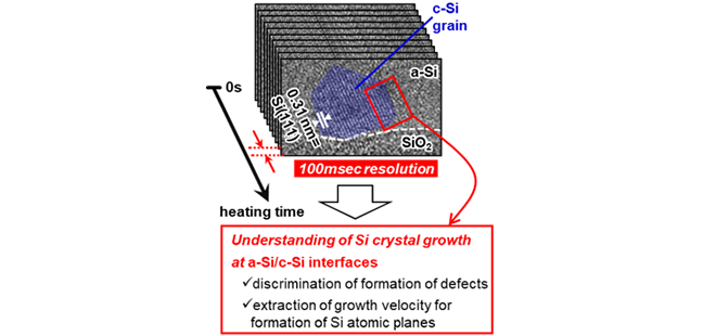
In 3D LSI, transistors are formed on polycrystalline Si (poly-Si). Poly-Si channels, which is the path for the current in this transistor, are key components in 3D LSI. Poly-Si channels with no defects are required for high-performance 3D LSI[1, 2]. Thus, the establishment of a formation process of poly-Si channels with no defects is one of the major challenges. To overcome this issue, we developed in situ transmission electron microscopy and investigated the crystal growth at the interface between amorphous Si (a-Si) and crystalline Si (c-Si), which is the basis of poly-Si formation. We successfully observed the continuous formation of Si atomic planes at a-Si/c-Si interfaces one by one (thickness of a single plane: 0.31 nm). As illustrated in Figure 1, the variation of lattice fringes of Si atomic plane under 823 K was continuously recorded with a time resolution of 100 ms, which enables us to discriminate the formation of defects, and to extract the growth velocity.

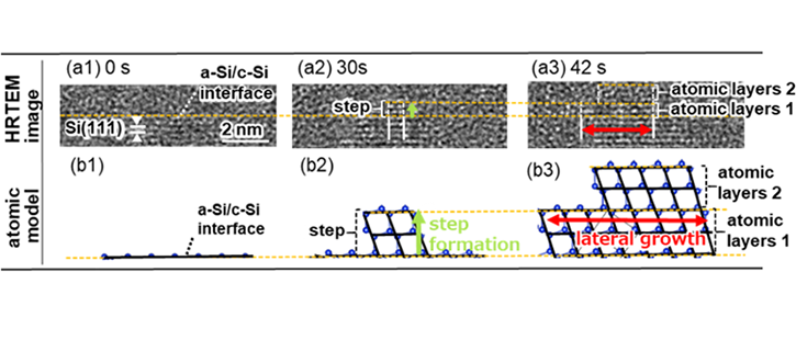
Figure 2 shows the elementary process of Si(111) formation at 823 K. First, the step is formed at the a-Si/c-Si interface (Fig.2(a2) and (b2)). Subsequently, lateral growth successively occurs across the surface of the crystal region, resulting in the formation of atomic layers (Fig.2(a3) and (b3)). These results showed the formation of defect-free Si crystals via ideal SPE growth.

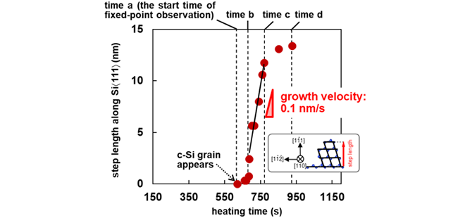
Figure 3 shows the variations in the step length along the <111> as a function of heating time during single c-Si grain growth. When the temperature is maintained at 823K for 619s, the c-Si grain appeared. Fixed-point observation was started at 619s (time a). Until the time b in Figure 3, the step length is almost constant. During further heating, the step length increases at a constant growth velocity (~0.1nm/s) as the grain size increases (Fig.3, time b–c). Then, the increase in the step length slows down because the grain gets closer to the other grains (Fig.3, time c–d). Thus, three stages in c-Si grain growth were directly observed, which had not been reported in conventional studies using X-ray diffraction, Raman spectroscopy.
These findings can be used in the development of process technology for the formation of defect-free poly-Si channel in 3D LSI.

This research has been presented at the 2022 International Conference on Solid State Devices and Materials.[3]
This article is reconstructed from excerpts of references [3] @2022 Japan Society of Applied Physics.
Reference
[1] M. Oda, K. Sakuma, Y. Kamimuta, and M. Saitoh, “Carrier Transport Analysis of High-Performance Poly-Si Nanowire Transistor Fabricated by Advanced SPC with Record-High Electron Mobility,” 2015 IEEE International Electron Devices Meeting, IEDM 2015, 125.
[2] T. Asano, R. Takaishi, M. Oda, K. Sakuma, M. Saitoh, and H. Tanaka, “Individual analysis of inter and intragrain defects in electrically characterized polycrystalline silicon nanowire TFTs by multicomponent dark-field imaging based on nanobeam electron diffraction two-dimensional mapping,” Japanese Journal of Applied Physics, 2018, vol. 57, 04FD20.
[3] M. Tezura, T. Asano, R. Takaishi, M. Tomita, M. Saitoh, and H. Tanaka, ”Real-Time and Atomic-Scale Observation of Local Solid-Phase Epitaxial Growth in Thin Silicon Film,”, 2022 International Conference on Solid State Devices and Materials, SSDM 2022, pp. 309-310.

