Please select your location and preferred language where available.
Thyristor Operation for High Speed Read / Program Performance in 3D Flash Memory with Highly Stacked WL-Layers
January 29, 2021
BiCS FLASH™ can increase its memory density and reduce the product cost by increasing the number of word line (WL) layers. However, it will increase the channel length and give rise to a higher series resistance, a smaller read current, and finally a read performance degradation. The thyristor structure is one of the promising candidates to obtain a large read current even the number of stacked layers is increased (ex. [1], [2]). This time, we closely examined the thyristor operation based on measurement data of 3D cell devices as well as TCAD simulations.
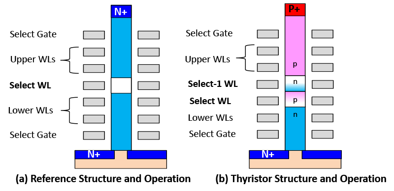
At both ends of the conventional cell, there are N type impurity regions (N+) which supply negative charge into the semiconductor channel (Fig. 1(a)). If the positive voltage applied to a selected WL induces negative charge in semiconductors, the channel is connected and becomes ON state. And if the negative charge is not induced, the channel is not connected and becomes OFF state.
On the other hand, in the thyristor cell, N+ region is located at the bottom of channel, and P type impurity region (P+) is at the top (Fig. 1(b)). Unselected WLs of lower side are applied positive voltage, and unselected WLs of upper side are applied negative voltage. In OFF state, the selected WL is applied negative voltage and constructs barrier for negative charge, and the adjacent WL (select-1 WL) is applied positive voltage and constructs barrier for positive charge. Then channel charges create virtual PNPN regions. This is a similar PNPN structure to the thyristor used as a switching device of power semiconductor devices. If the selected WL voltage exceeds the threshold, the potential barrier of thyristor suddenly collapses, and a large current can flows.

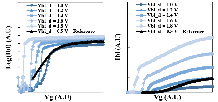
Figure 2 shows the memory cell current (Ibl) I-V characteristics of conventional and thyristor operation. Compared with conventional operation (thick black line), a steep current rise from OFF state to ON state is found in thyristor operation. Moreover the ON state current can be larger than the conventional operation.

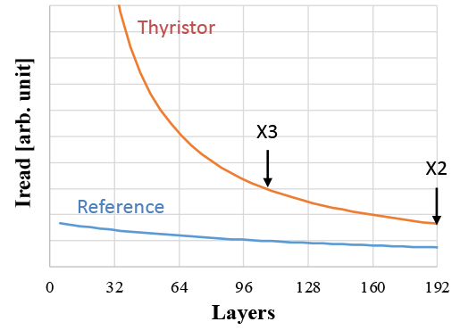
According to our estimation by TCAD simulation, if appropriate voltages are applied to each terminal, the thyristor operation can realize read current 2 times larger than that of conventional operation even WL stakes as many as about 200 layers (Fig. 3).

However, the original thyristor operation has a serious problem to be overcome. The strong cell-to-cell interference may change the Vth of a memory cell when the neighbor memory cell is programmed. This is because the positive charge barrier mentioned above is decreased. Therefore, to reduce cell-to-cell interference, the positive charge barrier must be reinforced so that it may not affect to the programming. However, even if we attempt to increase the barrier by raising WL voltage, there is an applicable maximum voltage of WL due to program disturbance. We have found a novel WL bias scheme that uses two WLs adjacent to selected WL. It can strengthen the positive barrier using the same voltage as the original thyristor operation. By introducing this operation we improved the read performance by 20 % and the programming performance by 15 % in QLC (4 bits per cell).
This achievement was presented in the International Memory Workshop (IMW2020), in May 2020[3].
[1] S.-M. Joe, H.-J. Kang, N. Choi, M. Kang, and B.-G. Park, IEEE Trans. Elec. Dev. Vol.63, No.4, 1533 (2016).
[2] N. C. Choi, H.-J. Kang, S.-H. Bae, B.-G. Park and J.-H. Lee, 2017 Symposium on VLSI Technology Digest of Technical Papers, T15-2 (2017).
[3] H. Horii, T. Maeda, and T. Sanuki, ” Thyristor Operation for High Speed Read/Program Performance in 3D Flash Memory with Highly Stacked WL-Layers” 2020 IEEE International Memory Workshop, IMW 2020 – Proceedings 9108147
This material is a partial excerpt and a reconstruction of the reference [3] © 2020 IEEE.
Company names, product names, and service names may be trademarks of their respective companies.

