Please select your location and preferred language where available.
A 25.6Gb/s Interface with Ring Topology for High-Bandwidth and Large-Capacity Storage Systems
March 06, 2020
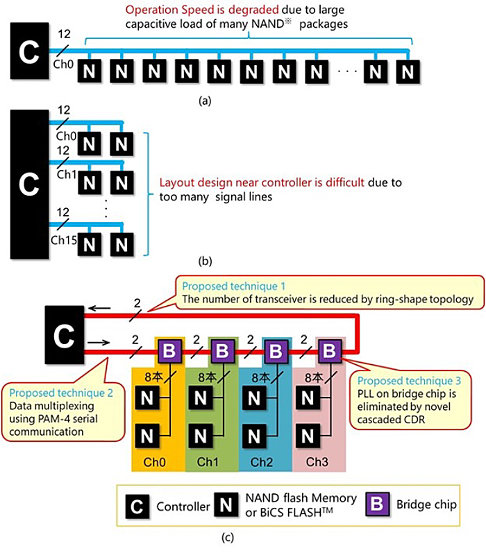
High-speed and large-capacity storages are increasingly required by various big-data applications such as medical and financial areas. In order to achieve a large-capacity storage using NAND Flash memory and BiCS FLASH™(hereinafter, referred to as NAND), many NAND packages have to be connected to a controller. However, the operation speed is degraded by large load capacitance due to the many NAND packages on a single channel as shown in Figure 1(a). On the other hand, if many channels are used to reduce the load capacitance per channel, the number of high-speed signal lines will increase and this will complicate the printed circuit board layout near the controller as shown in Figure 1(b).
To solve these issue, we have proposed a daisy-chain configuration*1 using bridge chips, to achieve high-speed operation and large capacity with fewer signal lines as shown in Figure 1(c) [1,2]. To reduce chip area and power consumption of the bridge chip, three techniques have been developed [2]. The first one is a technique to reduce the number of transceivers on the bridge chip from two to one by using ring–topology connection between controller and the bridge chips. The second one is a technique to lower the operation-speed in the bridge chips’ circuits in order to relax their required performance by using PAM4*2 serial communications compared to conventional NRZ*3 which utilizes only binary signal of 0 or 1. The final one is a technique to reduce chip area and power consumption by eliminating a PLL*4 circuit on the bridge chip using a new cascaded CDR*5 circuits with improved jitter*6 characteristics.

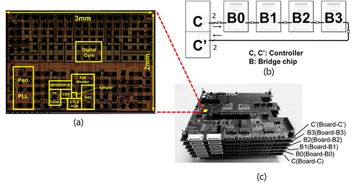
The die micrograph of the fabricated chip is shown in Figure 2(a). The bridge chip was fabricated in a 28nm CMOS process and it can act as both bridge chip and controller. The evaluations were performed connecting four bridge chips and two controllers as shown in Figure 2(b) and (c).

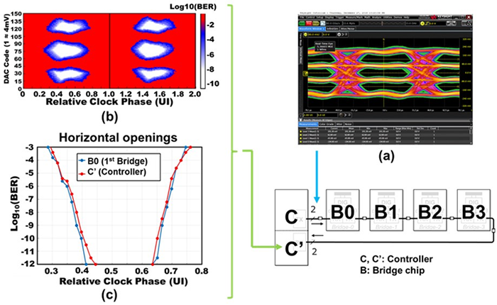
Figure 3(a) shows PAM4 signal output from the controller C measured by an oscilloscope, and a good PAM4 waveform is observed. This PAM4 signal is received by the final controller C’ via four bridge chips B0 – B3. Figure 3(b) shows an eye diagram*7 observed utilizing on-chip eye monitor on the final controller C’ and clear three eye openings for each cycle waveform are obtained. Figure 3(c) shows measured bit error rate (BER) of the bridge chip B0 and final controller C’, and sufficiently low BER less than 10-12 is obtained for both cases. By similar measurements for all chips in the daisy chain, we confirmed 25.6-Gbps PAM4 communications with sufficient performance for all bridge chips and controllers.

These results demonstrate a possibility of achieving high-speed and large-capacity storage using the bridge chip and were presented at the International Solid-State Circuits Conference 2019 (ISSCC 2019) in San-Francisco in February 2019 [2].
- NAND Flash Memory or BiCS FLASH™
- Daisy-chain configuration: A configuration of propagating signals along multiple devices connected in series.
- PAM4: 4-Level Pulse Amplitude Modulation
- NRZ(Non-return-to-zero): A binary code which does not return to zero volt for each bit
- PLL: Phase Locked Loop, a circuit to generate a reference signal
- CDR: Clock Data Recovery, a method to recover a clock signal from a received data signal
- Jitter: Fluctuation in the time domain of the clock or signal waveforms
- Eye Diagram: A graphically superimposed signal waveforms which are repetitively sampled
References
[1] Y. Tsubouchi, D. Miyashita, Y. Satoh, T. Toi, F. Tachibana, M. Morimoto, J. Wadatsumi, and J. Deguchi, “A 12.8 Gb/s Daisy Chain-Based Downlink I/F Employing Spectrally Compressed Multi-Band Multiplexing for High-Bandwidth and Large-Capacity Storage Systems,” 2018 Symposium on VLSI Circuits, pp. 149-150 (2018)
[2] T. Toi, J. Wadatsumi, H. Kobayashi, Y. Shimizu, Y. Satoh, M. Morimoto, R. Ito, M. Ashida, Y. Tsubouchi, M. Nozawa, G. Urakawa, and J. Deguchi, "A 25.6Gb/s Uplink-Downlink Interface Employing PAM-4-Based 4-Channel Multiplexing and Cascaded CDR Circuits in Ring Topology for High-Bandwidth and Large-Capacity Storage Systems", 2019 IEEE International Solid - State Circuits Conference - (ISSCC), pp. 478-480 (2019)

