Please select your location and preferred language where available.
Analytical Technologies for Next-Generation Devices
August 28, 2018
In order to achieve high-performance and high-functional next-generation memory devices, it is essentially required to have (1) device design and process technology for 3D nanostructures, (2) material technologies that can introduce various functional thin films, (3) analysis technology that can reveal device nanostructure and material composition.
As many 3D memory nanostructures consist of intricately stacked thin films, it is very important to accurately understand the nanostructures of individual films, the interfaces between them, and the elemental composition distribution in order to realize high-performance and high-reliability devices. New analytical techniques need to analyze nanometer-level 3D structures, and we are driving various advanced analysis methods to achieve this task.
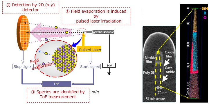
Specifically, Atom Probe Tomography (APT) can reveal 3D elemental distribution by counting the atoms one by one, as shown in the left figure. The right figure is an example of transistor (MOSFET) elemental analysis that can successfully visualize the 3D profile of elements on the nanometer level.


