Please select your location and preferred language where available.
Identification of key atomic process of the metal-induced lateral crystallization mechanism for channel in 3D flash memory using first-principles calculations
December 17, 2024
3D flash memory requires further stacking to meet market demands for higher bit density and larger capacity storage. However, the increased resistance due to longer poly-Si channels results in insufficient cell current. To address this challenge, Metal-induced Lateral Crystallization (MILC) technology has been developed to improve poly-Si channel mobility[1][2][3].
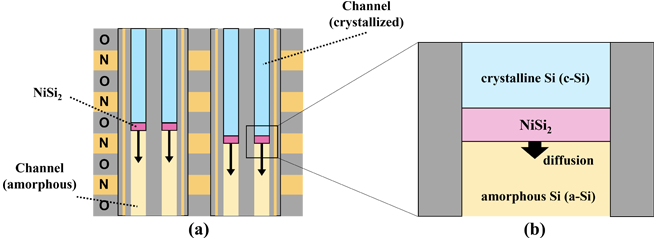
Figure 1(a) shows a schematic diagram of the crystallization process for memory holes using MILC. During the diffusion of NiSi2 grains from top to bottom of the channels, crystallization progresses through MILC. Figure 1(b) illustrates MILC phenomenon. NiSi2 grains diffuse through the amorphous Si (a-Si) channels due to annealing. After NiSi2 passes through, crystalline Si (c-Si) is left behind. In the MILC process, the channels are crystallized by diffusing NiSi2 before a-Si transforms into poly-Si.

While various experiments and theoretical calculations have been conducted on MILC, atomic-scale research has been limited to studies of crystal NiSi2 or the crystalline interface between c-Si and NiSi2 (c-Si/NiSi2 interface)[5]. A comprehensive understanding of the overall mechanism throughout one crystallization cycle, including the interface between NiSi2 and a-Si (NiSi2/a-Si interface), had not been achieved. To make MILC technology practical, crystallization efficiency must be significantly improved. However, it is difficult to establish improvement strategies without understanding the fundamental mechanism. Therefore, we investigated the atomic-scale and overall mechanism of MILC and what is the rate-limiting factor using first-principles calculations[4].
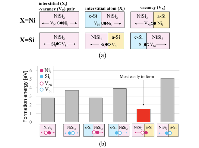
MILC is considered to be a phenomenon involving several factors such as complex interfaces, grain boundaries, and impurities in NiSi2. However, since NiSi2 itself does not change before or after diffusion, the essential factor is that Ni or Si atoms, or their vacancies, pass through the NiSi2 crystal. The diffusive species are possible to form in the NiSi2, at the c-Si/NiSi2 interface and NiSi2/a-Si interface. As a result, the six species shown in Figure 2(a) are candidates for diffusive species.
Figure 2(b) shows the formation energies required for these candidates. We were the first in the world to theoretically reveal that Ni vacancy, because of Ni moving from NiSi2 into a-Si, is the most easily formed and are the most dominant diffusion species in MILC.

Next, we investigated how Ni vacancy diffuses though NiSi2. Figure 3(a) shows the NiSi2 crystal structure with a Ni vacancy, showed by the dotted circle. When this Ni vacancy moves to the position of Ni atom A, some diffusion paths are possible. Our analysis revealed that a complex diffusion path involving four atomic sites, as shown in Figure 3(b), has the lowest energy barrier and is the most favorable for diffusion.

Finally, Ni vacancies diffusing through this complex path aggregate at the c-Si/NiSi2 interface. As Ni atoms are removed from NiSi2 during this process, the c-Si region expands[5]. Based on these results, one cycle of MILC phenomenon can be explained in three steps: Ni vacancies (1) form at the NiSi2/a-Si interface, (2) diffuse through NiSi2 via the complex paths, and (3) finally aggregate at the c-Si/NiSi2 interface, as shown in Figure 4(a). Understanding one cycle of MILC phenomenon allows us to identify the rate-limiting process by comparing the energies of these three steps.
Figure 4(b) shows the calculational values of the energy barriers required for each of the three steps. Step (2) has the highest energy barrier and is the slowest step. This value is consistent with the experimental value. Thus, we were the first in the world to theoretically identify step (2) as the bottleneck of MILC phenomenon.

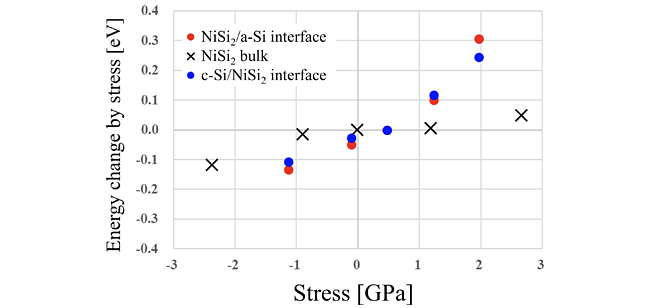
It is possible to evaluate the effect of stress on MILC with the fundamental mechanism clarified. The channel is embedded in 3D flash memory and is subject to stress from its surroundings. This study considered cases where a channel is subjected to compressive and tensile stress along the memory hole direction. Figure 5 shows the calculation results.
The horizontal axis stands for stress on the channel, with tensile stress on the negative direction and compressive stress on the positive direction. The vertical axis shows the difference in energy required for Ni vacancy diffusion compared to the stress-free value. This result shows that tensile stress reduces the energy for diffusion, potentially increasing MILC growth rate. This trend is consistent with previous experimental studies[7][8], supporting the proposed mechanism.

During chip manufacturing, channels are subject to various external influences, for example stress. By clarifying the mechanism, we can simulate how the external influences affect MILC. We will continue to contribute to accelerating development by proposing process improvements through principle-based simulations.
This achievement was presented at the international conference SISPAD 2024.
Reference
[1] H. Miyagawa et. al., “Metal-Assisted Solid-Phase Crystallization Process for Vertical Monocrystalline Si Channel in 3D Flash Memory”, 2019 IEEE International Electron Devices Meeting, pp.650-653.
[2] N. Ishihara et. al., “Highly Scalable Metal Induced Lateral Crystallization (MILC) Techniques for Vertical Si Channel in Ultra-High (> 300 Layers) 3D Flash Memory”, 2023 IEEE Symposium on VLSI Technology and Circuits, T7-1.
[3] Haruki Matsuo et. al., “Effects of crystallinity of silicon channels formed by two metal-induced lateral crystallization methods on the cell current distribution in NAND-type 3D flash memory”, Jpn. J. Appl. Phys. 2024, 63, 04SP19.
[4] Y. Ogawa et. al., “Identification of key atomic process of Metal-induced lateral crystallization from First-principles Calculations”, 2024 IEEE International Conference on Simulation of Semiconductor Processes and Devices, 1-3.
[5] J.-S. Ahn et. al., “Effect of MSi2/Si(111) (M = Co, Ni) interface structure on metal induced lateral crystallization”, Thin Solid Films 2013, 542, 426-429.
[6] G. Z. Radnóczi et. al., “Structural characterization of nanostructures grown by Ni metal induced lateral crystallization of amorphous-Si”, J. Appl. Phys. 2016, 119, 065303.
[7] C.-Y. Hou et. al., “Effects of Tensile Stress on Growth of Ni–Metal-Induced Lateral Crystallization of Amorphous Silicon”, Jpn. J. Appl. Phys. 2005, 44, 7327.
[8] S. Y. Huang et. al., “Effect of compressive stress on nickel-induced lateral crystallization of amorphous silicon thin films”, Thin Solid Films 2021, 520, 2984.

