Please select your location and preferred language where available.
Bonding Overlay Measurement Technology in CBA Process for 3D Flash Memory
April 24, 2024
We developed groundbreaking CBA (CMOS directly Bonded to Array) technology, wherein each CMOS wafer and cell array wafer is manufactured separately in its optimized condition and then bonded together to realize enhanced bit density and fast NAND I/O speed[1]. In the CBA process, mark patterns for overlay inspection are formed at the time of Cu pad formation, and after wafers are bonded to each other, the overlay accuracy between substrates is measured.

Considering the further improvement of wafer bonding overlay, it can be said that overlay measurement is better to be performed right after wafer bonding. Figure 2 shows a schematic diagram of two different Advanced Process Control (APC) feedback loops. APC Feedback 1 shows a feedback loop after bonding, and APC Feedback 2 shows a feedback loop from after Si grind.
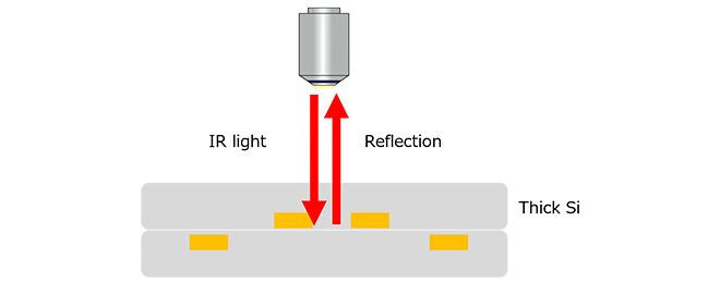
The former is easier to improve overlay than the latter because the turnaround time (TAT) of the feedback loop is shorter and the followability of process fluctuation is higher. However, the conventional overlay measurement tool using visible light cannot measure the overlay before Si grind, so we developed a new overlay measurement tool using IR in cooperation with KLA Corporation.

The Image Based Overlay (IBO) metrology tool is a reflection-based microscope using Short Wavelength Infrared (SWIR) with multiple spectral bands.

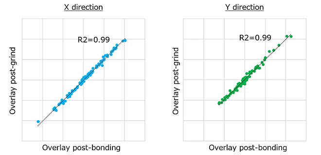
Figure 4 shows the results of the correlation value evaluated with the post-bonding overlay and post-Si grind overlay.

The correlation value between overlay of post-bonded and post-Si grind was around 0.99. The results show an excellent correlation between the post-bonding overlay and the overlay post-Si grind. This good correlation is an acceptable result when using a post-bonding overlay for APC.
This work was presented in the SPIE Advanced Lithography and Patterning 2024 in Feb.2024[2].
Reference
[1] S. Kobayashi et al., “High Performance 3D Flash Memory with 3.2Gbps Interface and 205MB/s Program Throughput based on CBA (CMOS Directly Bonded to Array) Technology”, 69th Annual IEEE International Electron Devices Meeting (2023)
[2] T. Goto et al., “Advanced overlay metrology for wafer bonding applications”, SPIE Advanced Lithography + Patterning 2024 Paper 12955-27

