Please select your location and preferred language where available.
Overview of new technologies applied to BiCS FLASH™ generation 8
March 28, 2024
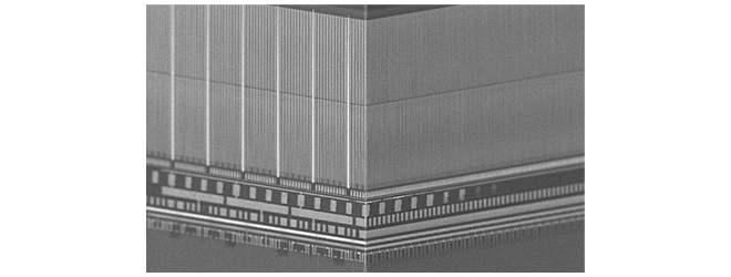
BiCS FLASH™ generation 8 is our latest high performance and high memory density 3D flash memory. Data are transferred to outside with 3.2Gbps speed, while data are read and programmed inside with 40μs time and 205MB/s throughput, respectively. With 218 world-lines stacked, the memory density of the 1Tb TLC (Triple Level Cell) product is well-scaled to 18.3Gb/mm2, which is the world’s highest in the 2xx (about 218-236) word-line stacked technology node. In order to enhance performance and the memory density, we applied the two new technologies, CBA (CMOS directly Bonded to Array) and OPS (On Pitch SGD), to BiCS FLASH™ generation 8 (Figure 1). The following is a brief introduction of the two technologies.

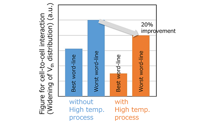
BiCS FLASH™ consists of the two components: the memory cell array where data are stored, and CMOS circuits which control the memory cell array. In the past technology node, CMOS circuits and the memory cell array are fabricated on a single wafer. Thus, applicable process conditions are limited, because favorable process conditions are different between the two. To address this issue, we developed CBA technology, where the two wafers are processed separately for CMOS circuits and the memory cell array, and are bonded afterwards. Since process conditions are optimized independently for CMOS circuits and the memory cell array, performance enhancement is expected in CBA. For example, we applied high temperature process during the memory cell fabrication in BiCS FLASH™ generation 8, which was not applicable to the non-CBA-type because of the severe degradation of CMOS performance, and minimized the electrical disturbance among the neighboring memory cells (Figure 2).

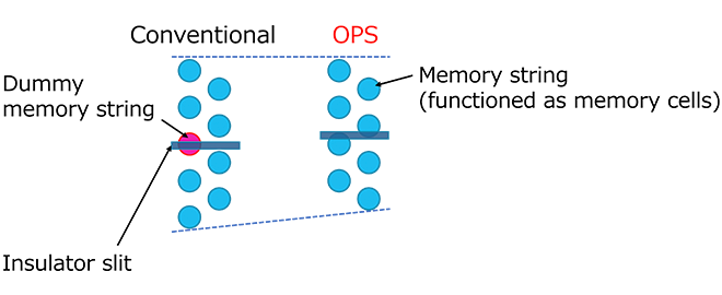
Next, we will explain OPS. The memory cell to access is uniquely selected, with the combination of voltage applied to word-line, bit-line, and select-gate in BiCS FLASH™. The select-gate is shared among the four lines of memory strings, and each select-gate is electrically separated by an insulator. When we look at the configuration of the select-gate and the memory strings in the in-plane direction, the insulator separating the select-gate (the insulator slit) overlaps with the dummy memory strings which do not function as memory cells in the past technology node. On the other hand, in OPS, the insulator slit is placed between the electrically active memory strings, and the dummy memory strings are eliminated to increase the memory density (Figure 3).
By adopting newly developed CBA and OPS technologies, we successfully enhanced performance and the memory density up to the level mentioned above in BiCS FLASH™ generation 8.

This achievement was presented at IEDM(International Electron Devices Meeting) 2023.
Reference
[1] M. Sako et al., “A 1Tb 3b/Cell 3D-Flash Memory of more than 17Gb/mm2 bit density with 3.2Gbps interface and 205MB/s program throughput”, Proc. IEEE Symp. VLSI Technol., Jun. 2023, C2-1.
[2] S. Kobayashi et al., “High Performance 3D Flash Memory with 3.2Gbps Interface and 205MB/s Program Throughput based on CBA(CMOS Directly Bonded to Array) Technology”, IEEE International Electron Devices Meeting (IEDM), Dec. 2023, 35-2.

