Please select your location and preferred language where available.
Development of CMOS Directly Bonded to Array(CBA) Technology for 3D Flash Memory
March 14, 2024
Recently, 3D stacked devices with copper (Cu) direct bonding process have been introduced in such as microprocessor and Complementary Metal Oxide Semiconductor(CMOS) image sensor to realize PPAC(performance, power, area, and cost)[1-4]. We have developed a new CMOS directly bonded to array(CBA) technology based on Cu direct bonding process and applied it to BiCS FLASH™ generation 8 to improve PPAC of 3D flash memory compared to the conventional technology.
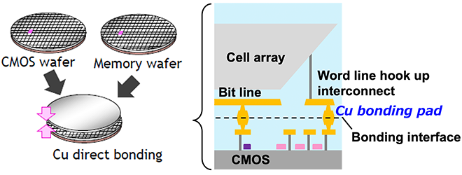
As shown in Figure 1, CBA technology consists of forming CMOS peripheral circuit (CMOS) and cell array on separate Si wafers, forming Cu bonding pads on each surface, and bonding between CMOS and cell array surfaces with Cu direct bonding process to fabricate 3D flash memory.
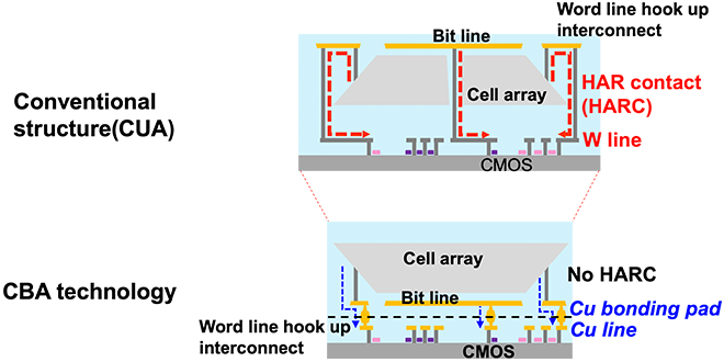
As shown in Figure 2, CBA technology eliminates high aspect ratio contacts(HARCs) which connect CMOS to cell array, and it is possible to use low resistance Cu line. In CMOS under Array(CUA) process, thermal budget during cell array formation restricts CMOS performance because cell array must be formed sequentially on CMOS. On the other hand, CBA technology can process both CMOS and cell array, individually. As results, CBA technology can reduce chip area and improve performance.
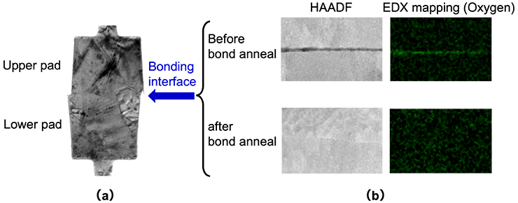
In CBA technology, Cu crystallinity of Cu bonding pad, surface topography during Cu-CMP process, surface condition of Cu bonding pad during bonding, alignment, and wafer warpage control were developed. As result, low resistance and high reliability Cu bonding pads without impurities such as oxygen at the pad interface, can be realized as shown in Figure 3.
©2023 IEEE[5]
*1 High Angle Annular Dark-Field
*2 Energy Dispersive X-ray Spectroscopy
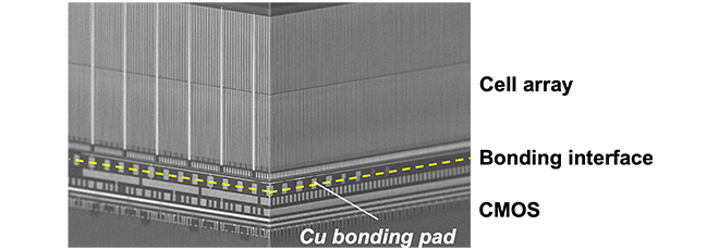
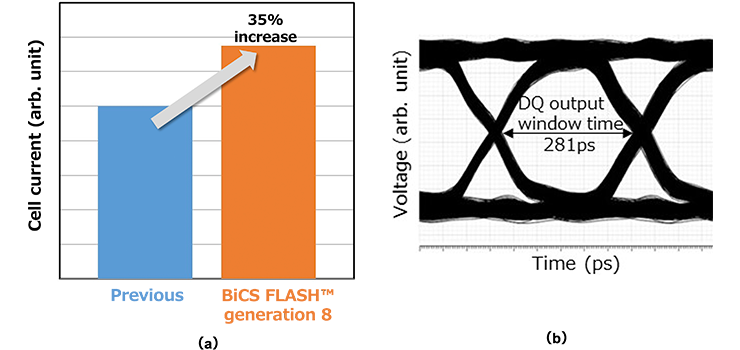
By applying this CBA technology to BiCS FLASH™ generation 8, we have realized 3D flash memory structure with 218-layered word lines as shown in Figure 4. Device performance achieved 35% higher cell current than conventional technology and interface speed achieved 3.2Gbps as shown in Figure 5. In near future, High-k/Metal Gate(HKMG) can be introduced in CMOS to further improve interface performance.
In addition, it will be possible to realize multi-stacked 3D flash memory with two or more CMOS and two or more cell arrays by advance CBA technology. CBA technology is promising to improve PPAC of 3D flash memory continuously in future.
This work was presented in the IEEE International Electron Devices Meeting 2023(IEEE IEDM 2023) in Dec. 2023[5].
Reference
[1] S. Arkalgud., “The Era of Advanced Packaging and Hybrid Bonding”, in Tutorial. 2022 IEEE International Electron Devices Meeting (IEDM).
[2] R. Agarwal et al., “3D Packaging for Heterogeneous Integration”, in Proc. 2022 IEEE 72nd Electronic Components and Technology Conference (ECTC)., pp. 1103-1107.
[3] Y. Kagawa et al., “Novel Stacked CMOS Image Sensor with Advanced Cu2Cu Hybrid Bonding”, in Proc. 2016 IEEE International Electron Devices Meeting (IEDM)., pp. 8.4.1-8.4.4.
[4] M. Sakakibara et al., “A Back-Illuminated Global-Shutter CMOS Image Sensor with Pixel-Parallel 14b Subthreshold ADC”, in Proc. 2018 IEEE International Solid-State Circuits Conference (ISSCC)., pp. 80-82.
[5] M. Tagami, “CMOS Directly Bonded to Array (CBA) Technology for Future 3D Flash Memory”, in Proc. 2023 IEEE International Electron Devices Meeting (IEDM).

