Please select your location and preferred language where available.
Cu dishing reduction on CBA process for 3D flash memory
December 26, 2023
In order to shrink chip size and increase the performance speed of 3D Flash memory, we have adopted CBA(CMOS directly Bonded to Array) process for the BiCS FLASH™ generation 8. In CBA process, CMOS(Complementary Metal Oxide Semiconductor) and memory cell array are fabricated on independent wafers separately, and finally connected through the Cu(copper) bonding pads formed on the surface of each wafer[1]. CBA realizes shortest wiring connection between CMOS and memory cell array, thus enabling further chip shrinkage. In addition, the thermal budget for CMOS can be optimized independently from the memory cell array formation process, enabling faster device speeds.
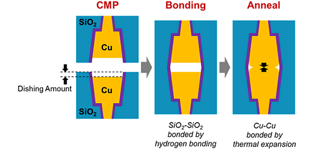
In CBA process, wafers are bonded together by forming hydrogen bonds between silicon oxide films, and then Cu-Cu junctions are formed by thermal expansion of Cu during annealing process (Figure 1). Therefore, it is necessary to reduce the dishing(Cu dent) amount formed during CMP(Chemical Mechanical Polishing) to less than the thermal expansion amount of Cu.

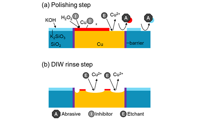
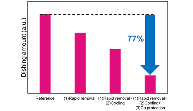
We proposed the hypothesis that dishing is enhanced by chemical etching during the DIW(De-ionized Water) rinse step after the polishing step (Figure 2). We considered that the etchants in the slurry remain after the polishing step, and etch Cu surface that is partially protected by inhibitors(Cu surface protectors) during the DIW rinse step. Based on the hypothesis, we proposed three approaches to reduce dishing: (1) rapid removal of etchant with a large amount of DIW, (2) suppression of chemical etching by cooling, and (3) enhancement of Cu surface protection with inhibitors, which successfully reduced the amount of dishing by 77% (Figure 3). We achieved good electrical yield of Cu-Cu junctions to be required for CBA technology with these approaches[2].


These results were presented at the international conference ICPT 2023.
Reference
[1] S. Sivaram and A. Ilkbahar, “Searching for Nonlinearity: Scaling Limits in NAND Flash”, 2023 IEEE Symposium on VLSI Technology and Circuits, PL2-2 (Plenary).
[2] T. Watanabe et al., “Cu dishing reduction on CBA (CMOS directly Bonded to Array) process for 3D flash memory”, 2023 International Conference on Planarization/CMP Technology(ICPT), O29.

