Please select your location and preferred language where available.
Metal Induced Lateral Crystallization (MILC) Techniques for Vertical Si Channel in highly stacked 3D Flash Memory
October 04, 2023
Abstract
The crystallization technology for Si channel, using metal-assisted materials, has been developed for 3D (three-dimensional) flash memory. It has successfully achieved cell array operation for the first time. This approach can reduce the density of grain boundaries in the Si channel, leading to reduction in trap density in Si channel compared to conventional polycrystalline Si channel. As a result, this technology can realize lower channel resistance, smaller RTN (random telegraphic noise) and narrower threshold voltage distribution in QLC (quadruple level cell) operation.
Introduction
The market demand for higher bit density and larger capacity in memory devices has been increasingly strong in recent years. In the case of 3D flash memory, this demand has been addressed by increasing the number of cell layers, reducing gate pitch, and increasing bit per cell. However, increase in channel resistance with increasing the number of stacked cell, and ensuring cell reliability during multi-level operation have emerged as key challenges. Development of the Metal-Induced-Lateral-Crystallization (MILC) technique has been pursued in order to overcome these challenges[1][2].
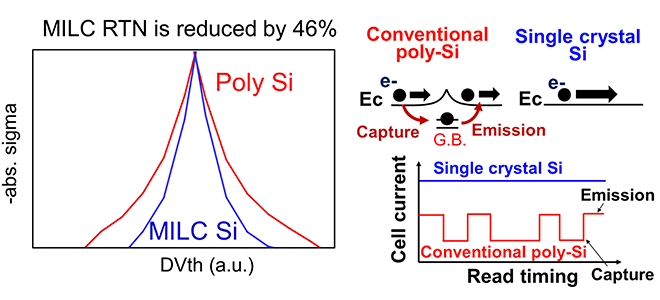
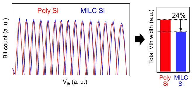
In this study, the MILC technique was utilized to successfully achieve channel single crystallization in a three-dimensional structure with up to 320 layers of word-lines (Figure 1), less than 1/10 reduction of channel resistance, over 40% reduction in random telegraph noise and 24% narrower threshold voltage distribution during QLC (quadruple level cell) operation [3].
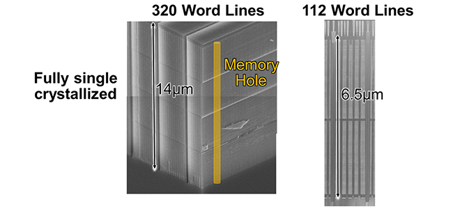
Single crystallized channel in highly stacked 3D structures using MILC technology
In the MILC technology, Ni silicide is diffused from the top to the bottom layer of the memory hole, thereby inducing the single crystallization of the Si channel (Figure 2). Any factors hindering the diffusion of Ni silicide along this path prevent the complete crystallization of the Si channel down to the bottom of the memory hole. In this study, the optimization of the deposition method for the Si channel layer and the thermal treatment for facilitating the diffusion of Ni silicide was conducted, leading to the successful suppression of inhibiting factors. Consequently, a macaroni-shaped Si channel[4] with a length of 14 μm, formed within a 320-layer memory hole, was fully single-crystallized (Figure 3).
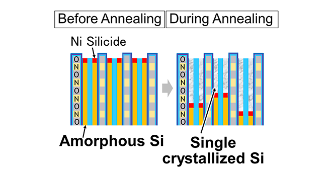
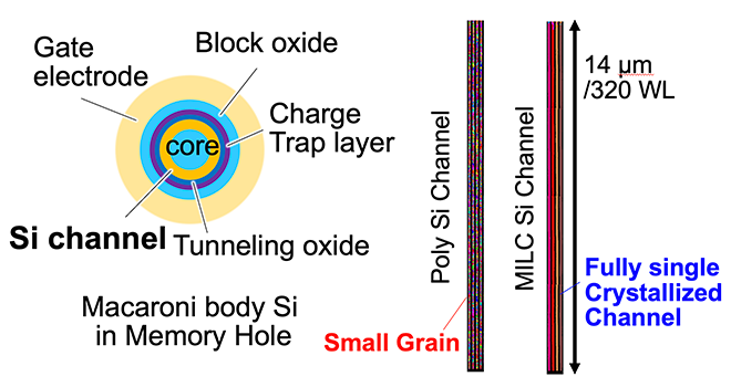
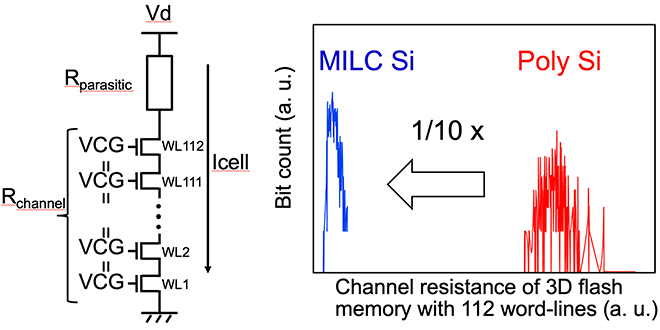
Improvement in channel resistance of 3D flash memory with MILC technique
Polycrystalline Si channels have many grain boundaries, and within which numerous lattice defects exist. These defects form electron trap site and become a source of electron scattering, which consequently increases channel resistance. Single-crystal Si channels with extremely reduced grain boundary density can be expected to reduce channel resistance significantly. Applying MILC single-crystal Si channels to 112-layer 3D Flash memory and confirmed from actual measurements that the channel resistance is reduced to approximately 1/10 compared to polycrystalline Si channels.
Improvement in multi-level cell operation of 3D flash memory with MILC Si channel
MILC single-crystal Si channels is also effective in reducing RTN (random telegraphic noise) caused by electron traps at grain boundaries in memory cell operation (Figure 5). RTN induces random fluctuations in threshold voltage of MOSFET (metal-oxide-semiconductor field-effect transistor) and degrades memory characteristics. With reducing RTN, a better QLC (quadruple level cell) operation has been confirmed with 24% reduction in the total width of threshold voltage distribution when compared to a polycrystalline Si channel (Figure 6).
Summary
The application of MILC single-crystalline Si channels to 3D flash memory enables us to realize approximately 10 times channel conductance, over 40% reduction in random telegraph noise, 24% narrower threshold voltage distribution in QLC operation through as compared to conventional polycrystalline Si channels. MILC single-crystalline Si channels have been demonstrated as a key technology for further 3D flash memory, facilitating higher layer stacking, increased bit density, and enhanced reliability.
This achievement was presented in the 2023 Symposium on VLSI Technology and Circuits [3].
Reference
[1] H. Miyagawa et. al., “Metal-Assisted Solid-Phase Crystallization Process for Vertical Monocrystalline Si Channel in 3D Flash Memory”, 2019 IEEE International Electron Devices Meeting, pp.650-653.
[2] S. Ramesh et. al., “Understanding the kinetics of Metal Induced Lateral Crystallization process to enhance the poly-Si channel quality and current conduction in 3-D NAND memory”, 2021 IEEE International Electron Devices Meeting, pp. 210-213.
[3] N. Ishihara et. al., “Highly Scalable Metal Induced Lateral Crystallization (MILC) Techniques for Vertical Si Channel in Ultra-High (> 300 Layers) 3D Flash Memory”, 2023 IEEE Symposium on VLSI Technology and Circuits, T7-1.
[4] Y. Fukuzumi et. al., “Optimal Integration and Characteristics of Vertical Array Devices for Ultra-High Density, Bit-Cost Scalable Flash Memory”, 2007 IEEE International Electron Devices Meeting, pp.449-452.

