Please select your location and preferred language where available.
Mechanism of adhesion between mold resin and copper in electromagnetic wave shield packages
November 9, 2022
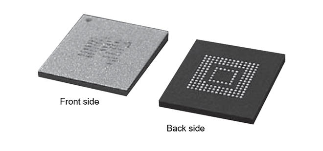
Many mobile devices such as smartphones contain semiconductor packages with built-in flash memory and a controller chip for controlling the flash memory. Radiation noise generated by the controller chip affects high-frequency circuits via the antenna and decreases the communication distance and data transmission speed via electromagnetic interference. Conventionally, to prevent this electromagnetic interference, metal plates (sheet metal shields) are used to cover multiple semiconductor packages. However, thinner mobile devices cannot accommodate sheet metal shields. To tackle this problem, we have developed an electromagnetic wave shield package in which the semiconductor package itself is covered with a metal film to provide shielding [1]. Figure 1 shows a photograph of the electromagnetic wave shield packages and Figure 2 shows a cross section of the electromagnetic wave shield package.
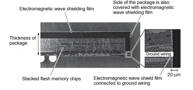
In addition to connecting the metal film to the copper wiring of the circuit board, the electromagnetic wave shield package must ensure adhesion between the mold resin that encapsulates the flash memory and the metal film that is formed later. The metal film is mainly made of copper and is deposited by the sputtering method used in the front-end process in semiconductor manufacturing.
In this study, we examined the adhesion mechanism between the mold resin and copper and found that the following two things are necessary to ensure adhesion [2].
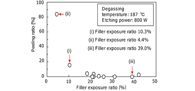
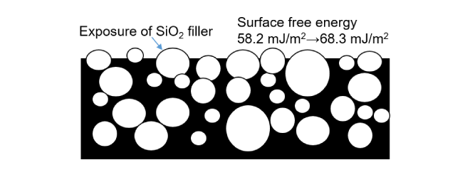
- It is necessary to plasma etch the resin components in the mold resin to expose the silica (SiO2) filler. Figure 3 shows the relationship between the amount of silica filler exposed on the mold resin surface on the horizontal axis and the delamination rate measured by the cross-cut method. The peeling ratio decreased as the silica filler exposure increased.
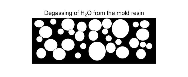
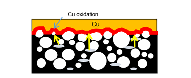
- Moisture absorption in the mold resin needs to be removed.
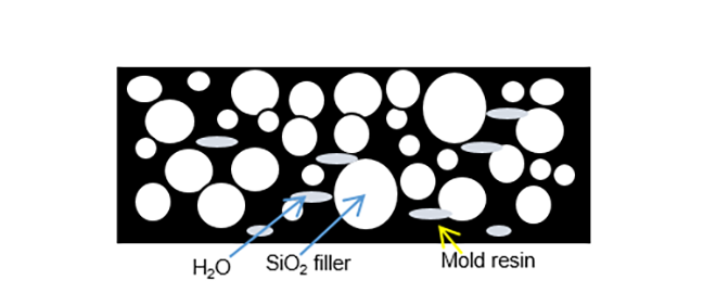
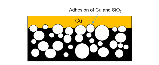
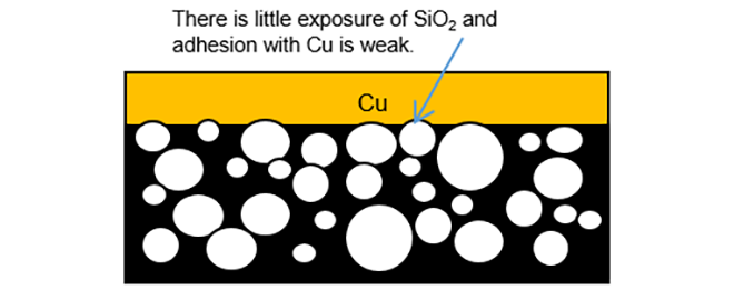
Our results suggest the following adhesion mechanism (Figure 4).
Fig.4 Adhesion mechanism between mold resin and sputtered copper [2]
We will continue to elucidate the adhesion mechanisms of different materials and develop processes for high value-added products that integrate the front-end and back-end (packaging) processes in semiconductor manufacturing.
This article is reconstructed from excerpts of references [1]@2016 Toshiba Review and [2]@2022 Thin Solid Films.
Reference
[1]H. Yamazaki, Y. Takano, and S. Honma, “Technology to Form EMI-Shielding Film on Semiconductor Packages Using Sputter Deposition”, Toshiba Review, 2016, vol. 71, no. 6, pp. 16-19.
[2] S. Homma, M. Shima, Y. Takano, T. Watanabe, K. Murakami, M. Fukuda, T. Imoto, and H. Nishikawa. “Adhesion mechanism between mold resin and sputtered copper for electromagnetic wave shield packages”, Thin Solid Films, 2022, vol. 750, 139188.

