Please select your location and preferred language where available.
Predictive analysis of the electrical failure with defect information in manufacturing processes
February 24, 2022
In recent years, the structures of semiconductor devices are complicated and there are some which require several months until a product is completed through many manufacturing processes. The products are shipped what did the strict electric test and passed. If there are some chips rejected by the test, analytical investigations are performed immediately for the rejected products to take measures against problems. However, defective products will be continued until an abnormal unit is fixed. Therefore, we do many production line (in-line) monitors to detect defects such as a dust and an abnormal pattern’s shape in the middle of processes. The defects are classified into categories like a dust, an open or a short of circuit pattern using the high resolution’s images of SEM*1, and then the improvement of the abnormal process unit which is specified by the category is made. Classification work is automated by deep learning now, and the system which improves the health of a production line for a short time is built. Moreover, although in-line defective data (a category, coordinates, size) is used also for the electric test’s pass rate (rejection rate) prediction, it was a subject the predictive accuracy was low in some in-line monitors.
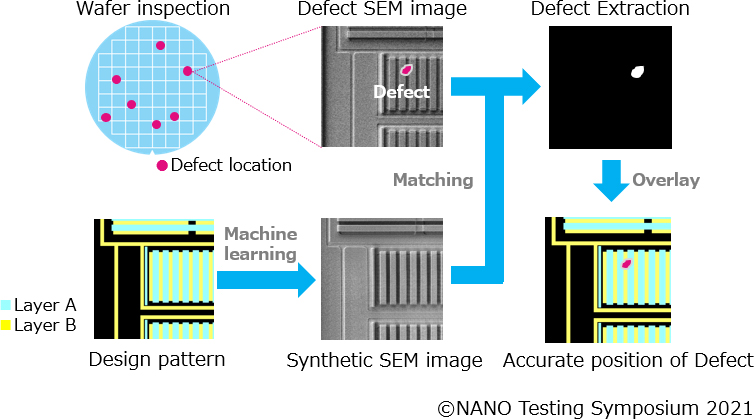
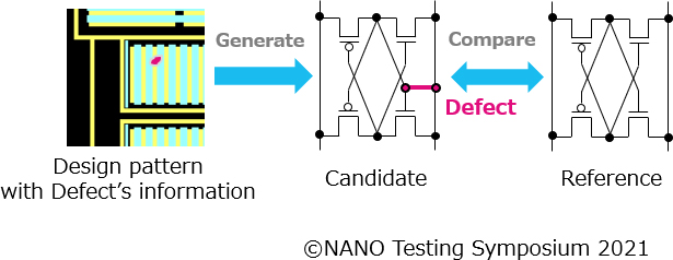
We work on digitalization of in-line defective data and design layout data for the improvement in predictive accuracy this time. First, as shown in Fig. 1, the synthetic SEM image of the normal pattern is generated from the design layout (CAD*2) using machine learning[1], and it becomes possible to extract highly precise defective information (coordinates and region) by comparing with the SEM image of the defect. Next, an electric diagram is created using LVS*3 which is one of the design verification tools from this defective information and a design layout, and the pass or rejection of an electric test is judged (Fig. 2). With the proposal technique, it succeeded in improving the above mentioned predictive accuracy from 56% to 73%. We integrate the sophisticated defect inspection equipment technology and digital processing technology, and also continue to promote the advancement of a smart factory.


The international conference "SPIE (The International Society for Optical Engineering) Advanced Lithography 2021" on semiconductor patterning technology announced this result [2][3].
- Scanning Electron Microscope
- Computer Aided Design
- Layout vs Schematic
Reference
[1] T. Ohashi, Y. Konno, A. Nakajima, C. Ida, A. Hamaguchi, “A study of lithography process prediction using GAN”, NANO Testing Symposium 2019
[2] J. Okude, C. Ida, K. Nojima, A. Hamaguchi, “In-line schematic failure analysis technique by defect SEM images”, Proceedings of SPIE - The International Society for Optical Engineering, 11611, 116110M
[3] J. Okude, C. Ida, K. Nojima, A. Hamaguchi, “In-line schematic failure analysis technique by fewer frame defect SEM images”, NANO Testing Symposium 2021

