Please select your location and preferred language where available.
High-density 3D flash memory using high-precision wafer bonding brings new value to storage
Kioxia's 8th generation BiCS FLASH 3D flash memory makes the most of CBA technology
Reprinted from: EE Times Japan
Reprinted from content published in EE Times Japan on July 30, 2024
This content is used with permission from EE Times Japan.
Department names and titles are as of the time of the interview.
Flash memory is becoming increasingly more important as a result of the exponential growth of data
In recent years, the amount of data being generated has skyrocketed as a result of the automation of a wide variety of systems, the electrification of automobiles and the rise of generative AI. In order to process such large amounts of data, high-performance processors are being developed and adopted very quickly. In this context, NAND flash memory (hereinafter “flash memory”) plays an increasingly crucial role.
As the amount of data increases, so does the need for flash memory, which is used for storing data and applications. This increased demand has helped drive the evolution of flash memory in terms of larger capacity, improved read/write performance, reduced power consumption, and faster interfaces speed.
In order to meet these market demands, KIOXIA has been developing technologies to increase the capacity and density of flash memory.
The KIOXIA approach to develop flash memory goes beyond mere reliance on vertical scaling
Faithful to its mission of “Uplifting the World with ‘Memory’”, KIOXIA invented flash memory in 1987. For nearly 40 years, KIOXIA has been a leader in the development of flash memory technology.
The first flash memory evolved in two-dimensions (lateral scaling). As memory cell array line and space scaling technology advanced, memory capacity and memory density per silicon die gradually improved. Scaling became a source of competition among flash memory manufacturers, but the limit was reached when the memory cell array line and space hit the 15nm process. This was due to a growing number of issues that could no longer be ignored, including the fact that memory cells become too close to each other causing current leakage, or that the number of electrons stored in a memory cell decreases, affecting read/write performance reliability.
The next step in the evolution of flash memory consisted of stacking memory cells in three dimensions (vertical scaling). Increasing the number of layers causes the number of memory cells per unit area to increase, resulting in higher capacity and integration. In 2007, KIOXIA announced the 3D flash memory technology for the stacking memory cells. In 2015, KIOXIA commercialized a 48-layer 3D flash memory under the BiCS FLASH brand name*1. Since then, KIOXIA has released BiCS FLASH products approximately every two years with increasing number of layers. In 2021, KIOXIA released the 6th generation of BiCS FLASH, consisting of 162 layers.
In recent years, flash memory manufacturers have focused primarily on developing technologies to increase the number of layers of memory cells and increase memory density. Each time a new generation of flash memory is released, the number of layers increases with some products boasting more than 200 layers. However, as Atsushi Inoue, Vice President of Memory Division at KIOXIA, explained, "Increasing the layers of memory cells is only one way of increasing capacity and memory density, and we are not exclusively preoccupied with the number of layers."
Increasing the number of layers of memory cells poses many challenges in terms of cost and manufacturing processes. The most obvious one is the increased difficulty of manufacturing process. Extremely deep and fine holes need to be etched with high precision through a stack of extremely thin layers in order to form the memory cells. This requires the use of cutting-edge equipment, which causes manufacturing costs to skyrocket. The more memory cell layers in a stack, the longer the production time.
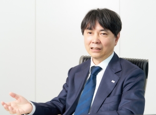
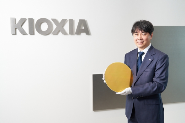
Atsushi Inoue, Vice President of Memory Division at KIOXIA
According to Inoue, "For KIOXIA, the most important aspect of making 3D flash memory is how to efficiently increase the integration and density of memory cells. What is important is how many gigabytes can be created on a single wafer, in other words, the ability to increase gigabyte density (GB/mm2). Rather than simply increasing the number of stacked layers, our approach consists of ensuring the best balance between cost and performance by optimizing factors such as memory hole depth, lateral scaling technology, and process technology."
The latest flash memory developed with this design philosophy is the 218-layer 8th generation BiCS FLASH*2. This latest generation will be produced at the KIOXIA Yokkaichi plant (Yokkaichi City, Mie Prefecture) and Kitakami plant (Kitakami City, Iwate Prefecture).
With CBA, control circuits and memory cells are created on separate wafers
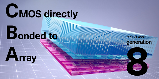
The most distinctive feature of 8th generation BiCS FLASH is the introduction of a technology called "CMOS Directly Bonded to Array (CBA) ". It involves creating the CMOS circuitry that controls the memory cells and the memory cell array on separate wafers, then inverting the wafer with the memory cell array and bonding the two wafers together.
For the previous 6th generation of BiCS FLASH, CMOS Under Array (CUA) technology was used in the manufacturing process. The CUA process involved making a cell array on top of a previously made CMOS circuit and then performing high-temperature annealing to improve the reliability of the memory cells. However, high-temperature processing has a negative impact on the performance characteristics of the transistors in the CMOS circuit. As a result, the CUA manufacturing process was subject to significant temperature restrictions, creating a hurdles to further improving memory cell performance.
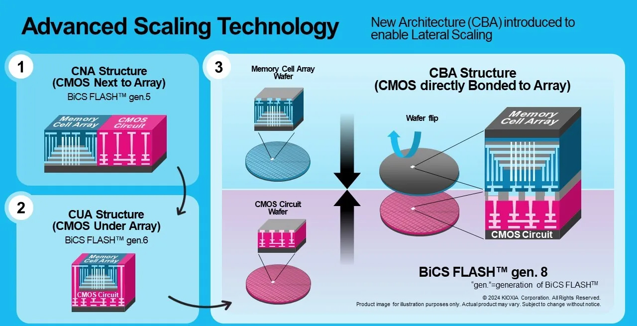
Overview of CBA technology used in 8th generation BiCS FLASH. (Source: KIOXIA)
The advantage of CBA technology is that the CMOS circuit wafers and memory cells array wafers can be manufactured separately. Performing high-temperature processing solely on the memory cell array wafer makes it possible to achieve the optimal temperature to ensure reliability without having to consider the impact on the CMOS circuit. By separating the wafer manufacturing processes, the performance of the CMOS circuit and the memory cell array can be maximized.
Since the two types of wafers are manufactured in parallel, there is also the added benefit of shortened production times compared to the conventional method.
However, bonding the wafers together is not an easy feat. In order to ensure the reliability of flash memory, extremely precise alignment is required in the bonding process. "If you assume a wafer diameter of 1 km, the accuracy required to bond the wafers together would be in the order of 1 mm or less," says Inoue. Poor bonding alignment accuracy may prevent the product from functioning as flash memory or may significantly reduce the product’s lifespan and reliability.
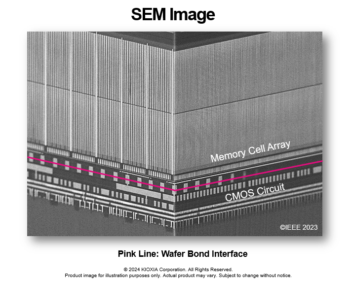
The above photograph of an 8th generation BiCS FLASH was taken with an electron microscope. The pink lines indicate the smooth bonding surface, with the memory cell array on top and the CMOS circuit on the bottom. Another distinctive feature is that the pitch is just a few microns wide. (Source: KIOXIA)
In order to smoothly bond the two wafers together, the surfaces of each wafer must be very flat, and sophisticated processing is required to flatten them. CBA technology is the result of a series of advanced technologies coming together in the manufacturing process to produce the 8th generation BiCS FLASH.
8th generation BiCS FLASH has 218 layers, more than the previous generation. “This means about 5% fewer layers than competing products of the same generation (e.g., 3D flash memories with approximately 230 layers). However, our calculations tell us that gigabyte density is about 15 to 20% higher. Which makes me think that our method achieves higher integration more efficiently," concludes Inoue.
8th generation BiCS FLASH represents a significant advancement both in terms of density and performance. Gigabyte density has increased by 50% compared to the previous generation of BiCS FLASH. Write performance has improved by 20%, and read speed has increased by 10%. Power consumption has been reduced by 30% (during write operation). Interface speed is 3.6 Gbps*3 (gigabits per second). "The adoption of CBA has improved the characteristics of the memory cell itself, which has directly led to improvements in write performance and other areas," says Inoue.
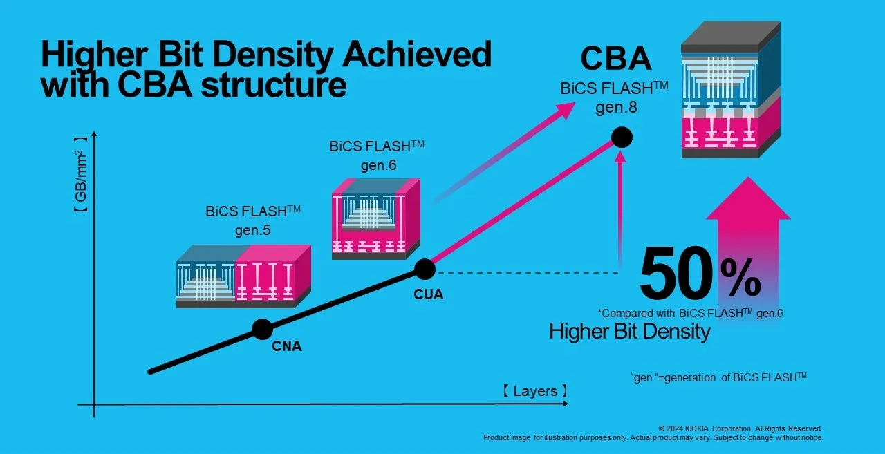
The adoption of CBA and related technologies has led to a significant increase in gigabyte density in the 8th generation of BiCS FLASH. (Source: KIOXIA)
"It's not really that easy to improve performance by this much," says Inoue. "Generally speaking, as the number of stacked layers increases, each layer becomes thinner and the memory cell becomes smaller, which negatively affects the elementary characteristics of the memory cell. Unless you overcome this problem, and at the same time create a highly reliable cell, you won't see any improvement in performance. I think this is an area where memory vendors are struggling. Even so, improving performance by about 10% with each new generation is a worthy goal and indicator of success."
"Improving memory density by increasing the number of layers is one of several effective approaches,” says Inoue. “However, it is important to innovate by introducing the most appropriate technology for a particular time, such as CBA, rather than relying on the number of layers. We believe that the 8th generation of BiCS FLASH is the embodiment of that approach."
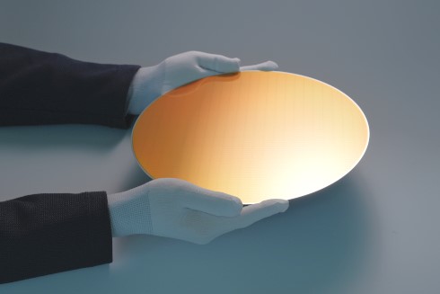
300mm wafer of the 8th generation of BiCS FLASH
Increasing demand for SSDs in Data Centers
8th generation BiCS FLASH is suitable for a wide range of applications, from PCI Express 5.0 (PCIe Gen 5) SSDs, which are increasingly being installed in PCs, to smartphone storage, data center SSDs, enterprise SSDs, and in-vehicle storage. "We have received positive feedback in terms of reliability and performance from customers to whom we have shipped samples," says Inoue.
In particular, they are expected to be widely used in data centers. "High bandwidth memory (HBM), which is increasingly being used in data center servers as a result of the advent of generative AI, consumes very high amounts of power. This generates a growing need for low-power, small, lightweight SSDs," says Inoue. In the enterprise field, too, KIOXIA expects HDDs to be replaced by SSDs at ever higher speed.
"We will continue to work with our partners to create a better society and continue to develop high-density flash memory with improved performance in order to expand their horizon."
As the number of applications generating massive amounts of data increases, the importance of flash memory as a way to store the world’s data will continue to grow. The 8th generation of KIOXIA's BiCS FLASH 3D flash memory will no doubt add new value to today’s storage applications.
Notes
- The information described on this article is at the time of interview and may not be the most up-to-date.
- "BiCS FLASH" is a trademark of KIOXIA Corporation.
- The 8th generation BiCS FLASH referred to in this article is 1Tb TLC (Triple Level Cell) product.
- 1Gbps is calculated as 1,000,000,000bits/second. This value is obtained under specific Kioxia’s test environment, and may vary depending on the user’s conditions.
