Please select your location and preferred language where available.
Toshiba Launches New Embedded NAND Flash Memory Modules Using 19nm Second Generation Process Technology
New Products Compliant with JEDEC e・MMC™ Version 5.0
- October 31, 2013
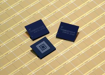
TOKYO—Toshiba Corporation (TOKYO: 6502) today announced the launch of new embedded NAND flash memory modules integrating NAND chips fabricated with 19nm second generation process technology. The module is fully compliant with the latest e•MMCTM [1] standard, and is designed for application in a wide range of digital consumer products, including smartphones, tablet PCs and digital video cameras. Mass production will start from the end of November.

Demand continues to grow for large density NAND flash memory chips that can support high resolution video and deliver enhanced storage. This is particularly true in the area of embedded memories with a controller function, which minimize development requirements and ease integration into system designs. Toshiba is meeting this demand by reinforcing its line-up of high density memory products.
The company’s new 32-gigabyte (GB) embedded device integrates four 64Gbit (equal to 8GB) NAND chips fabricated with Toshiba's cutting-edge 19nm second generation process technology and a dedicated controller into a small package measuring only 11.5 x 13 x 1.0mm. It is compliant with JEDEC e・MMCTM Version 5.0, published by JEDEC in September, and achieves a high read/write performance by applying the new HS400 high speed interface standard.
Toshiba will bring the NAND chips to a line-up of single-package embedded NAND flash memories in densities from 4GB to 128GB. All will integrate a controller to manage basic control functions for NAND applications.
New Product Line-up
Product Name |
Capacity |
Package |
Mass Production |
|---|---|---|---|
THGBMBG8D4KBAIR |
32GB |
153Ball FBGA 11.5x13x1.0mm |
End of November, 2013 |
THGBMBG7D2KBAIL |
16GB |
153Ball FBGA 11.5x13x0.8mm |
End of November, 2013 |
Following 16GB and 32GB products, Toshiba will release 4GB, 8GB, 64GB and 128GB products in turn.
Key Features
- The JEDEC e•MMCTM V5.0 compliant interface handles essential functions, including writing block management, error correction and driver software. It simplifies system development, allowing manufacturers to minimize development costs and speed up time to market for new and upgraded products.
- Embedded in a system, the 128GB module can record up to 2,222 hours of music at a 128Kbps bit rate, 16.6 hours of full spec high definition video and 38.4 hours of standard definition video[2].
- The new products apply NAND flash memory chips fabricated with leading-edge 19nm second generation process technology.
- The new products are sealed in a small FBGA package measuring just 11.5 x 13mm and has a signal layout compliant with the JEDEC e•MMCTM V5.0.
Key Specifications
Product Name |
THGBMBG8D4KBAIR |
THGBMBG7D2KBAIL |
|
|---|---|---|---|
Interface |
JEDEC e•MMCTM V5.0 standard HS-MMC interface |
||
Capacity |
32GB |
16GB |
|
Power Supply Voltage |
2.7~3.6V (Memory core) 1.7V~1.95V / 2.7V~3.6V (Interface) |
||
Bus Width |
x1 / x4 / x8 |
||
Write Speed |
90MB per sec. (Sequential/HS400 Mode) |
50MB per sec. (Sequential/HS400 Mode) |
|
Read Speed |
270MB per sec. (Sequential/HS400 Mode) |
270MB per sec. (Sequential/HS400 Mode) |
|
Temperature Range |
-25degrees to +85degees Celsius |
||
Package |
153Ball FBGA 11.5x13x1.0mm |
153Ball FBGA 11.5x13x0.8mm |
|
Notes:
[1] e•MMCTM is a trademark and a product category for a class of embedded memory products built to the JEDEC e•MMCTM Standard specification.
[2] HD and SD are calculated at average bit rates of 17Mbps and 7Mbps, respectively.