Please select your location and preferred language where available.
Kioxia and MoDeCH Develop a Three-Dimensional Probing System
High-Frequency Characteristic Measurement for Three-Dimensional Structures up to 110 GHz
- September 27, 2024
- Kioxia Corporation
- MoDeCH Inc.
Kioxia Corporation, a world leader in memory solutions, and MoDeCH Inc., a leading developer of modeling and design technology, announced the development of an industry first probing system for high-frequency characteristic measurement for three-dimensional (3D) objects up to 110 GHz at The European Microwave Conference (EuMC) on September 26(1).
Conventionally, solid-state drives (SSDs) in data centers are inserted into high-speed interface connectors on the processor motherboards. In this situation, transmission lines for high-speed interfaces such as PCIe® adopt a 3D structure that extends from the motherboards of the processor to the printed circuit boards (PCBs) in the SSDs via orthogonal card-edge connectors (Figure 1). High-frequency characteristics of such 3D structures are typically evaluated by simulations. With the newly developed 3D probing system, it is now possible for the first time to directly measure characteristics of 3D structures up to 110 GHz.
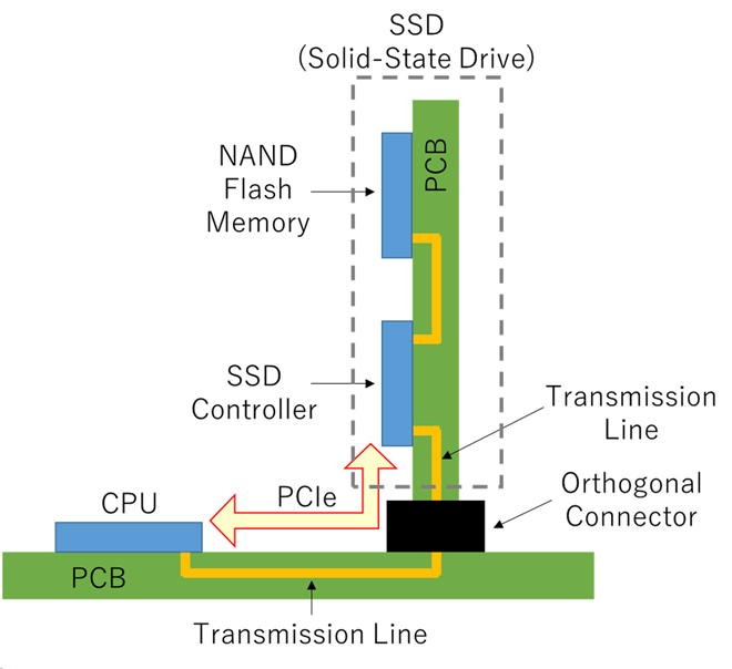
Figure 1: 3D transmission line between processors and SSDs ©2024 EuMA
Kioxia and MoDeCH developed a 3D probe station to measure high-frequency characteristics of the 3D structure (Figure 2). The station incorporates a built-in mechanism that rotates high-frequency probes and frequency extenders together, making contact with a 3D structure in order to measure it.
In addition, the companies developed thru standards for individual 3D structures (Figure 3) for accurate measurement of high-frequency characteristics. To evaluate a vertically bent 3D structure, a thru was created on a flexible substrate that was bent vertically using a jig and fixed in place to create a standard thru.
Using the developed 3D probing system and the thru standard for the 3D structure, the newly developed 3D probing system successfully measured high-frequency characteristics of two transmission lines up to 110 GHz on the two PCBs that were connected using the orthogonal connector (Figure 4).
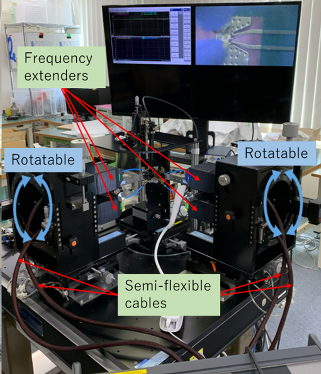
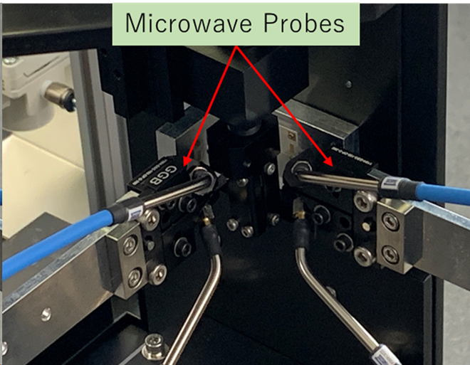
Figure 2: Photographs of developed 3D probe station ©2024 EuMA
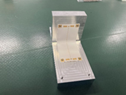
Figure 3: Thru standard for orthogonal 3D structures ©2024 EuMA
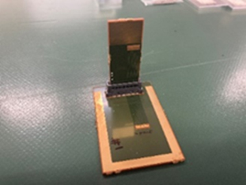
Figure 4: 3D test structure including two transmission lines and one orthogonal connector ©2024 EuMA
This industry-first development is a result of the “Research and Development Project of the Enhanced Infrastructures for Post 5G Information and Communication Systems” (JPNP 20017), commissioned by the New Energy and Industrial Technology Development Organization (NEDO).
Notes
- Y. Sakuraba et al., “A 110-GHz Probing System for S-parameter Measurements of Three-Dimensional Objects,” European Microwave Conference 2024 (EuMC 2024), EuMC46-4
Images used in this press release come from this thesis.
- Company names, product names, and service names may be trademarks of third-party companies.
Information in this document, including product prices and specifications, content of services and contact information, is correct on the date of the announcement but is subject to change without prior notice.